Graphene: Why the Nobel Prize and Why Raman?
Graphene has potential applications ranging from computer monitors to solar cells, and Raman spectroscopy is a useful method for its characterization.


Graphene, which consists of single layers of perfectly crystalline graphite, was first reported in Science in 2004 (1). It was were created by the "highly sophisticated" technique of peeling off layers of highly oriented pyrolytic graphite (HOPG). One might imagine that Geim and Novoselov and their colleagues were simply searching for a new interesting material, interesting due to the physical properties resulting from its two-dimensional nature. However, reading the original 2004 publication, one realizes that the study was motivated by the goal to identify a semiconducting material with properties that could enable continued miniaturization of microelectronics when the limits of silicon's properties are reached.
The function of microelectronics is based on the electric field effect; this means that by applying an electric field, one can alter the free carriers — and consequently the electric current — flowing through the device. In the 2004 Science article Novoselov and Geim pointed out that very thin metallic films also had the potential to exhibit the field effect, but it had never been demonstrated because thin metallic films are mechanically unstable and become discontinuous. It had also been predicted that graphene layers would be unstable, forming curved surfaces; but undaunted, Geim and Novoselov charged forward, peeling off thin layers of graphene, depositing them on SiO2 on Si, and then making measurements showing that the field effect does exist in this material. The Nobel Prize in Physics announcement stated that Novoselov and Geim showed "that carbon in such a flat form has exceptional properties that originate from the remarkable world of quantum physics."
Graphene Properties and Potential Uses
Five years after the original Science article, Geim published a review in Science summarizing much of what followed the 2004 report (2). Current densities have been measured at six orders of magnitude higher than copper; electrons move with zero effective mass, over micrometer distances without scattering, even at room temperature, in films decorated with adsorbates. This means that quantum effects survive at room temperature, with implications for engineered applications. Graphene is the thinnest, yet strongest, material known, being both brittle and ductile simultaneously. And in its purest form it is impermeable to even He, the smallest gas known. Based on these properties, numerous possibilities have been proposed and tried.
For electronics, one important targeted goal is the fabrication of high-electron-mobility transistors (HMETs); these devices, which are widely used in communication technologies, have been based on GaAs, but graphene is of particular interest because it offers the possibility of extending the range to terahertz frequencies. Geim's 2009 review summarizes the results up to the time of his writing.
The Nobel Prize announcement lists an interesting set of other applications (3). Such possibilities include paper-thin computer monitors that can be rolled up; transparent touch screens, light panels, and solar cells; plastics that can conduct electricity and heat with mechanical robustness (for uses in cars, airplanes, and satellites); and chemical sensors (made with surface adsorbates or channels). Clearly this column installment cannot address all of these possibilities in detail, but they are mentioned to motivate the application of Raman measurements to the characterization of materials being developed for these new exotic applications.
Raman Spectra of Graphene
The literature is full of publications dealing with the Raman effect in graphene. As a result of its structure and electronic properties, the Raman effect is quite interesting. As an introduction to the field, we recommend several reviews, starting with the review of the scattering process in graphite.
In their 2004 article, "Raman Spectroscopy of Graphite" (4), Reich and Thomsen developed a rigorous description of the Raman effect in graphite that is important for our understanding of the effect in graphene. Most important was their description of the double resonance phenomenon, which explained the excitation dependence of the "disorder" D band, the overtone spectrum, and the asymmetry of the Stokes/anti-Stokes scattering. In a perfect graphite lattice only the G band is observed near 1580 cm-1. In an imperfect lattice the D band is usually observed between 1330 and 1370 cm-1 when the spectrum is excited with a visible laser. What Reich and Thomsen showed is that this band is a vibration near a high symmetry K point of the Brillouin zone that appears in the spectrum following a double resonant process, which is why it is dependent on the excitation wavelength. The lattice defect is required to observe this band, because the double resonance with a single phonon requires a defect to take up the extra momentum of the scattering process. On the other hand, in a second-order process, no defect is required for the scattering to occur because the two phonons provide momenta for the two scattering events.
In 2004, Ferrari (5) used the double resonance formalism to focus on the Raman effect in graphene. The most striking differences between the spectra of graphene and graphite are the relative intensities of the G to 2D bands and the structure of the 2D envelope, both exhibiting effects as a function of number of layers. For single-layer graphene, the 2D band is sharp and roughly four times the intensity of the G band, whereas in graphite the 2D band has two components with roughly one-half and one-fourth the intensity of the G band. The 2D band can be followed as a function of excitation wavelength. It is seen to evolve from a single band from one layer, to four bands from two to four layers, and then the two bands, indistinguishable from those of graphite, from five or more layers; as the number of layers changes, the relative contributions of the four components change. In addition, Ferrari points out that partial screening of atomic vibrations by electrons at the Fermi surface (Kohn's anomaly) contributes to the dispersion of the D phonon energy with excitation wavelength.
An important question to answer is why two layers exhibit a 2D band with four components. Because the phonon splitting in two layers is known to be small, the answer lies in electronic band effects. The graphene planes interact causing the π and π* bands to split into four bands, with different splittings for electrons and holes. The result will be four doubly resonant processes that will be reflected in four phonon components in the 2D envelope.
When graphene is doped, the free carriers have effects on the spectra as well. The frequency of the G band increases with doping, regardless of the sign of the dopants. On the other hand, for the 2D band (or bands), high hole doping will produce phonon stiffening, and high electron doping will produce phonon softening. The doping level can be estimated by monitoring both spectral effects. In addition, the 2D band intensity will decrease with doping.
Ferrari also notes that graphene edges represent defects in that the lattice is interrupted. If the laser excitation spot overlaps an edge, the D band will be observed. This will be relevant when looking at graphene ribbons, where phonon and electron confinement can also be an issue. Note that because graphene has been proposed as a material for planar integrated circuits, these phenomena can be useful in characterizing materials during development, or ultimately during manufacturing.
In 2009 the Dresselhaus group also published a good review of this area (6), expanding on the details of the spectroscopy and the practical implications. They considered in more detail the scattering from different numbers of graphene layers. While group theoretical considerations confirmed the expected presence of four bands in the 2D (G' in their notation) region of bilayer graphene, similar calculations for trilayer graphene predict the presence of 15 layers. In fact, their trilayer spectra were adequately fit with six bands, always maintaining the 24-cm-1 Lorentzian width to define a characteristic lifetime for the doubly resonant process. Their four-layer spectrum was fit to three bands, but the behavior was clearly approaching that of graphite, with the highest intensity on the high frequency side. Another important observation concerns the behavior of turbostratic graphite. Unlike high quality graphite where the planes stack in a Bernal AB fashion, the successive planes in turbostratic graphite are randomly oriented in the plane and none of the group theory considerations for interplanar interactions will hold, at least on an averaged basis. In turbostratic graphite the 2D band is fit as a single Lorentzian, but with FWHM of 45–60 cm-1. From there, Dresselhaus and colleagues developed methods to determine the out-of-plane stacking order and in-plane crystallite size, parameters that will become important when developing microelectronic devices. By following the behavior of the 2D band of graphite films as a function of heat treatment (2200–2700 °C), they showed that the structure evolved from turbostratic to graphitic. Band-fitting these spectra enables estimating the volume composition of the 2D vs. the 3D composition from which, in combination with X-ray diffraction data, an experimental value for the c-axis lattice constant and the c-axis crystallite size Lc can be predicted from the Raman data.
What is really extraordinary is that, with rigorous understanding and modeling of the electron–phonon interaction in graphene, information on the electronic states can be extracted from these Raman spectra. The Kohn anomaly, mentioned earlier, explains the electronic screening of the phonons that gives rise to phonon renormalization. In the doubly resonant processes of graphene these electronic states are at the Fermi level; if the Fermi level is changed by doping or applying an external voltage, then the phonon renormalization will change, which can be observed as a frequency shift. Because of the larger electron phonon interaction for the G band, this band has been followed experimentally, and the results were presented in the Dresselhaus review. While some of the predictions have been confirmed, others have not, and it has yet to be determined if the model or the quality of the samples is the source of the discrepancies. Clearly, this information will be essential in engineering microelectronic devices based on graphene.
We noted above that Raman scattering from an edge of a perfect graphene plane will have intensity in the D band due to the effective loss of crystalline perfection at the edge. Cancado and colleagues (7) showed that differences in intensity of the D band from a zigzag vs. armchair edge can be attributed to differences in scattering wavevector at the two edges and how these wavevectors achieve the double resonance responsible for the intensity of this band.
Yoon and colleagues (8) studied the polarization dependence of the Raman signal and found that the 2D band signal is maximized when the laser and Raman polarization are parallel, and the G band is isotropic.
The Thomsen group (9) studied the splitting of the 2D band when graphene is subjected to strain. The splitting depends on the strength and direction of the applied stress, and the intensity depends on the polarization of the Raman and scattered photons relative to the graphene lattice directions. They predict that strain in the zigzag direction produces a larger splitting than strain along the armchair direction and plot frequencies confirming these predictions. A publication of a group from Columbia University shows the spectra as a function of polarization condition relative to the strain axis, and as a function of the angle between the strain axis and the polarization axis (10). This group also offers interpretation of these results involving electronic states.
Charged impurities lead to doping, which also has been documented to affect the Raman spectra. Casiraghi and colleagues (11) showed that even in samples not intentionally doped and with high structural order (vanishing D band intensity), the frequency of the G band can shift, and its FWHM increase, in the presence of doping. Caridad and colleagues (12) showed that unintentional doping in graphene on SiO2 is determined by the distance between the graphene sheet and the substrate.
Chemical Vapor Deposition Manufacture of Graphene Films
The real challenge facing the implementation of graphene-based microelectronics will be in the controlled manufacture of high quality planes at selected sites. Clearly the tape-pulling method has a limited future for manufacturing. Dresselhaus and colleagues reviewed the results of several methods used to deposit films of graphene. Surfaces of two hexagonal polytypes of SiC, 4H, and 6H have been graphitized — ABAC stacking occurs on 4H, and ABCACB is formed on 6H. There is a buffer layer of sp3 carbon at the interface, and the number of graphene layers is determined by the temperature (1200–1600 °C) and time of the heat treatment process. For best Raman analysis the films are transferred to SiO2 surfaces, and then using the information summarized above, the structure of the films can be inferred. Of interest is one study that showed that with a 300-nm laser spot, the width of the 2D band was about 25 cm-1, a value close to that of exfoliated graphene layers (13). In this study, spectra from three spots showed spectra with two values for the 2D frequency, which was interpreted as strain in the sample.
A second method of growth is chemical vapor deposition (CVD) on transition metals. For instance, Ni, with an in-plane (111) lattice constant of 0.232 nm, is well-matched to graphite (α = 0.246 nm) (mismatch of 5.6%) to enable growth of one and two layer domains as large as 20 μm in size. The intensity of the D band can be used to infer subdomain boundaries. Linewidths and frequencies of the thinnest layers demonstrate the presence of single-layer graphene. However, in layers determined by atomic force microscopy (AFM) to be two or three graphene sheets, a frequency and width of the 2D band consistent with single graphene layers implies that the layers are not stacked in the normal AB sequence and also that the electronic states are not coupled to the vibrations.
Graphene Nanoribbons
To engineer robust transistors with high on/off ratios using graphene, an energy gap must be designed into the material that normally is a zero gap semiconductor. Nanoribbons whose short dimension is in the range of a few nanometers will experience a gap in the electronic wavefunctions due to confinement. The size of the gap depends on the width of the ribbon and its chirality. At the time that the Dresselhaus review was written, not too many Raman studies of nanoribbons had been published. However, theoretical calculations have been published predicting the electronic and vibrational properties. These calculations will form the basis for interpretation of future Raman spectra, which will then provide assistance in the engineering of microelectronics. For example, heat treatment of nanoribbons (up to 2800 °C), in conjunction with transmission electron microscopy (TEM)–scanning tunneling microscopy (STM) images, has demonstrated the ability of Raman microscopy to follow the annealing process as seen in the significant reduction of the D band (14) in the ribbons. In particular, these observations give insight not only to the development of order in the ribbon, but also to the presence of edge loops, as evidenced by residual D band intensity.
Chemically Modified Graphene
Clearly this column cannot review the entire graphene literature, which is evolving quite rapidly. The goal has been to indicate the importance of the Raman measurements to this emerging field. There is one more topic that I want to cover, however, and that is some work that has been done on chemical modifications to graphene.
One remarkable modification has been the hydrogenation of graphene to graphane (15). It was found that graphane retains the hexagonal structure of graphene, but with an inhomogeneous, lattice compression. The hydrogenated samples were found to be doped with holes (as determined by Hall measurements) and were stable over time, but they could be restored to the conducting state by annealing. But electrical measurements showed that the material remained p-doped after annealing. Raman measurements corroborated the findings from the electrical measurements; note that all features arise from sp2 -hybridized carbon so the conclusion that the exposure to H produces sp3 carbon means that it is not fully hydrogenated. Hydrogenation produced D and D' (1620-cm-1 ) bands, a broadening and decrease in intensity of the 2D band, and the appearance of a D+D' band at 2950 cm-1, all of which is consistent with the breakdown of translational symmetry. In the annealed material D, D', and D+D' peaks were suppressed, but some details in the spectra indicated that the annealed graphene was p-doped.
Another well-known material is graphene oxide, which was first discovered in the mid-19th century and is formed by treating graphite with strong oxidizing agents. The formation of epoxide and hydroxyl groups results in almost doubling the interlayer spacing; rapid heating releases CO2, which then separates the graphite oxide (GO) to functionalized single graphene (FGS) sheets. Kudin and colleagues (16) investigated the Raman spectra of GO and FGS. The spectra showed significantly broadened G and D bands, with frequency shifts and asymmetry of the G band relative to that of graphite. These results are discussed in terms of specific types of five-, seven-, and eight-membered ring defects.


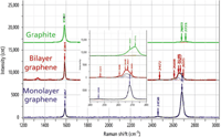
Figure 1: Raman spectrum of graphite, monolayer graphene, and bilayer graphene.
What Do Raman Spectra and Maps Look Like?
Figure 1 shows typical spectra of graphite, monolayer graphene, and bilayer graphene. The intense 2D band is seen in the spectrum of the single layer. In the bilayer material, the 2D spectrum is fit to four bands, and in graphite it is fit to two, as described earlier in this column. The bilayer spectrum shows some residual signal near 1340 cm-1, indicating the presence of some disorder in the material from which this spectrum was generated.


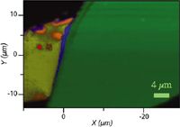
Figure 2: Raman map of overlapping graphene sheets. Each color represents regions where spectra were distinguishable.
Figure 2 shows a map of several overlapping flakes of graphene, generated from the 2D signal. A spectrum was recorded at each data point, and then the modeling function of the LabSpec software (Horiba Scientific, Edison, New Jersey) was used to extract unique spectra. These spectra are shown in Figure 3; each spectrum was band-fit to a combined Lorentzian-Gaussian function. Using the types of information implicit in the Raman spectra that were reviewed in this column, it can be seen that information on the physical state of a sample at the local level can be extracted without making electrical measurements. This will clearly be invaluable for the engineering and manufacturing of electronic devices.

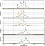
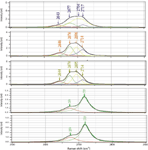
Figure 3: Modeled spectra of the 2D bands of each region shown in Figure 2. The spectra were band-fit to aid in characterizing each region.
Concluding Remarks
One of my previous columns discussed a variety of carbon materials, but in light of the attention now being paid to graphene, I thought it would be useful to go into more detail on this important new material. I have reviewed some of the Raman literature to evaluate the potential of Raman measurements to assist in characterizing graphene and then engineering its use into new electronic devices. My apologies to anyone whose publications have been overlooked. This column is not meant to be an exhaustive review of the literature, but an attempt to explain some of the characteristics of graphene's Raman spectrum that will aid in engineering its applications, in particular to microelectronics.


Fran Adar
Fran Adar is the Worldwide Raman Applications Manager for Horiba Jobin Yvon (Edison, New Jersey). She can be reached by e-mail at fran.adar@horiba.com.
References
(1) K.S. Novoselov, A.K. Geim, S.V. Morozov, D. Jiang, Y. Zhang, S.V. Dubonos, I.V. Grigorieva, and A.A. Firsov, Science 306, 666–669 (2004).
(2) A.K. Geim, Science 324, 1530–1535 (2009).
(3) Graphene – the perfect atomic lattice, HTTP://KVA.SE
(4) S. Reich and C. Thomsen, Phil. Trans. R. Soc. Lond. A 363, 2271–2288 (2004).
(5) A.C. Ferrari, Solid State Commun. 143, 47–57 (2007).
(6) L.M. Malard, M.A. Pimenta, G. Dresselhaus, and M.S. Dres-selhaus, Physics Reports 473, 51–87 (2009).
(7) L.G. Cancado, M.A. Pimenta, B.R. Neves, M.S. Dantas, and A. Jorio, Phys. Rev. Lett. 93, 247401 (2004).
(8) D. Yoon, H. Moon, Y.-W. Son, G. Samsonidze, B.H. Park, J.B. Kim, Y.P. Lee, and H. Cheong, Nano Lett. 8(12), 4270–4274 (2008).
(9) M. Mohr, J. Maultzsch, and C. Thomsen, Phys. Rev. B 82, 201409 (2010).
(10) M. Huang, J. Yan, T.F. Heinz, and J. Hone, Nano Lett. 10, 4074–4079 (2010).
(11) C. Casiraghi, S. Pisana, K.S. Novoselov, A.K. Geim, and A.C. Ferrari, Appl. Phys. Lett. 91, 233108 (2007).
(12) J.M. Caridad, F. Rosella, V. Bellani, M. Maicas, M. Patrini, and E. Diez, J. Appl. Phys. 108, 084321 (2010).
(13) J.A. Robinson, C.P. Pulls, N.E. Staley, J. Stitt, M.A. Fanton, K.V. Emtsev, T. Seyller, and Y. Liu, Nano Lett. 9, 964–968 (2009).
(14) J. Campos-Delgado, Y.A. Kim, T. Hayashi, A. Morelos- Gomez, M. Hofmann, H. Muramatsuu, M. Edo, H. Terrones, R.D. Shull, M.S. Dresselhau and M. Terrones, Chem. Phys. Lett. 469, 177–182 (2009).
(15) D.C. Elias, R.R. Nair, T.M.G. Mohiuddin, S.V Morozov, P. Blake, M.P. Halsall, A.C. Ferrari, D.W. Boukhvalov, M.I. Katsnelson, A.K. Geim, and K.S. Novoselov, Science 323, 610-613 (30 Jan 2009).
(16) K.N. Kudin, B. Ozbas, H.C. Schniepp, R.K. Prud'jomme, I.A. Aksay, and R. Car, Nana Lett. 8(1), 36–41 (2008).


Nanometer-Scale Studies Using Tip Enhanced Raman Spectroscopy
February 8th 2013Volker Deckert, the winner of the 2013 Charles Mann Award, is advancing the use of tip enhanced Raman spectroscopy (TERS) to push the lateral resolution of vibrational spectroscopy well below the Abbe limit, to achieve single-molecule sensitivity. Because the tip can be moved with sub-nanometer precision, structural information with unmatched spatial resolution can be achieved without the need of specific labels.


