Raman Crystallography
Polarization/orientation micro-Raman spectroscopy promises to be an important analytical tool to complement micro-X-ray diffraction.


Polarization/orientation (P/O) micro-Raman spectroscopy can be used to identify vibrational modes, determine crystal structure, distinguish allotropes and polymorphs, differentiate single from polycrystalline materials, and determine orientation of the crystal and degree of disorder, all on a micrometer scale. P/O micro-Raman spectroscopy promises to be an important analytical tool because of its complementarity to micro-X-ray diffraction. Here, we explain the theoretical basis for P/O micro-Raman spectroscopy and provide an example to demonstrate its feasibility.
In the February 2012 installment of this column (1), my colleague Fran Adar discussed the characterization of nanomaterials by Raman spectroscopy, noting that it is a method frequently used to differentiate amorphous from crystalline phases of a material. In this installment, I extend Fran's treatment of phonon spectroscopy by discussing the application of group theory to the Raman spectroscopy of crystalline materials. I cover the theory and general application of polarization/orientation (P/O) micro-Raman spectroscopy based on the interdependence of incident electric field, the Raman polarizability tensor dictated by the symmetry point group of the crystal, and the scattering vector. The method is quite complementary to X-ray diffraction and has been applied to microelectronic and photonic devices and other spatially heterogeneous structures. The application described also is valid for ionic solids (such as BaF2 or MgCl2), covalent solids (such as TiO2 or LiNbO3), and molecular crystals.
The title of this installment is inspired by that of the wonderful little book by Elizabeth Wood published in 1964, Crystals and Light: An Introduction to Optical Crystallography (2). This superb book on polarized light microscopy for the analysis of crystals is an extremely helpful companion to anyone performing polarized micro-Raman spectroscopy. (Of course, the incident laser light is always polarized; we use the term polarized strictly to refer to the selection of the polarization of the Raman scattered light.)
I do not intend to suggest that polarized micro-Raman spectroscopy is competitive with X-ray diffraction; it is not. Rather, where spatial variation of chemical composition or crystalline structure is on a scale or has a morphology that precludes or makes impractical the use of X-ray diffraction, polarized micro-Raman spectroscopy often can obtain crystallographic information. The scope of applications include the characterization of minerals, integrated electronics, photonic devices, microelectromechanical systems (MEMS), and the now heavily researched area of organic electronic devices including organic light-emitting diodes (OLEDs), photovoltaics, and field effect transistors. One particularly useful application of the P/O micro-Raman method is for the characterization of texture, such as of spatially varying grains, domains, or crystal orientation in natural or fabricated structures.
The dependence of Raman scattering on the masses of the constituent atoms and their bond strengths makes Raman scattering a good method for chemical analysis, and that is the application with which most spectroscopists are familiar. However, Raman spectroscopy can be used for the characterization of the atomic structure of solids because Raman scattering depends on the polarization and direction of the incident light, the crystal symmetry and orientation of the solid sample, and the direction and polarization of the collected scattered light. For example, micro-Raman spectroscopic methods for determining local crystal orientation in silicon have been developed to take advantage of these properties (3,4).
The discussion below explains the theory and gives an example of a more general application of P/O micro-Raman spectroscopy in the backscattering mode based on the interdependence of incident electric field, the polarizability tensor dictated by the symmetry point groups of the crystal class, and the scattering vector. Here we use the example of silicon, but the interested reader can find very elegant applications of the method to characterize GaN (5), sapphire (6), and zirconia (7).
The Example of Si: The Theory
To understand how P/O micro-Raman spectroscopy can be applied to the characterization of crystals, we begin by considering the most fundamental expressions related to Raman scattering:


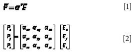
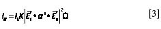
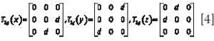
where α' is the Raman polarizability tensor representing the vibrational modulation of the polarizability, ε-bar is the incident electric field vector, and ρ-bar is the time-varying dipole moment (also a vector) induced by the interaction of the incident electric field with the vibrationally modulated polarizability of the material. The Raman polarizability tensor is fixed relative to the positions of the atoms and the directions of the bonds between them. Therefore, for a crystal fixed in space, the relationship described by equation 1 is dependent on the crystal symmetry and the orientation of the sample relative to the direction and polarization of the incident and collected light. This relationship constitutes that part of the expression for Raman scattering intensity of interest to us here, as follows:


where IR is the Raman scattering intensity, IL is the intensity of the incident light, K is a factor incorporating the dependence on the frequency of the incident light and the standard cross section, Ei the polarization of the incident light, and Es and Ω are the polarization and solid angle, respectively, at which scattered light is collected. The significance of this expression for work with crystals is that Raman scattering intensity is proportional to the square of the dot product of the incident electric field vector, Raman polarizability tensor, and scattering vector. Of great importance is that the forms (whether elements are zero or nonzero) of the polarizability tensors for crystals are dictated by the symmetry point groups of the crystal class to which the material belongs. The absolute magnitude of the tensor elements will be dictated by the specific chemical bonds between the atoms. However, whether a tensor element is zero or nonzero is entirely dictated by the crystal symmetry. There are 32 crystal classes and the forms of the Raman tensors have been determined for all of them and tabulated in various publications (8,9).
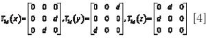
The most common crystalline form of Si is cubic, with two atoms in the primitive cell and crystal class Oh. The first-order optical phonon at 520 cm-1 is triply degenerate and there are three T2g Raman tensors of the form

An experimental arrangement can be envisioned in which the laser beam is incident along the x-axis and polarized along the y-axis, a single crystal Si(100) chip is positioned in the yz plane and backscattered light is collected in two configurations with the analyzer either parallel or perpendicular to the y-axis. Raman scattering strengths (normalized) have been calculated for the analyzer parallel and perpendicular to the incident polarization, given that the crystal is rotated in the yz plane. The calculated P/O diagram for Raman backscattering signal strength from Si(100) is shown in Figure 1. The parallel and perpendicular responses are sinusoidal functions 45° out of phase, and of course because of the cubic symmetry, the response is the same for the (010) and (001) faces. However, if the crystal is oriented out of these planes, one begins to see the effect of orientation on the P/O plots. The method used to transform the Raman polarizability tensors from one crystal orientation to another is the transformation through Eulerian angles (10). For example, Raman signals for the same experimental parallel and perpendicular configurations rotated 180° in the Si(110) plane were calculated and the results are shown in Figure 2. The P/O diagram for Si(110) is distinct from Si(100) and these crystal faces are easily differentiated.

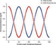
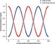
Figure 1: Calculated results for a P/O micro-Raman backscattering experiment for Si(100).
We have done P/O micro-Raman calculations for many other crystal orientations and have found the method to be very sensitive to crystalline Si orientation. In fact, this capability will be true for all crystals because the Raman responses of the P/O diagrams depend only on the form of the tensor, which is dictated by the crystal symmetry, and not the absolute magnitudes of the tensor elements dictated by the chemical bonding. Crystals of lower symmetry can have Raman tensors in which the nonzero elements are not equal, and in those cases the form of the P/O diagrams will be affected by the relative magnitudes of the tensor elements. In fact, fitting calculated P/O diagrams to the experimentally obtained P/O plots allows one to infer relative Raman scattering cross-sections from crystals. That the form or pattern of P/O diagrams is dependent on crystal symmetry, and not the specific elemental, compositional, or molecular identity of the crystal, is the basis for Raman crystallography. Calculations and experiments for other crystal classes and compounds have been performed in our laboratory, but we limit our discussion here to the Oh cubic crystal class and experimental results with Si to demonstrate the efficacy of this method.

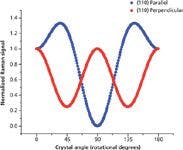
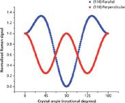
Figure 2: Calculated results for a P/O micro-Raman backscattering experiment for Si(110).
The discussion above establishes the theoretical basis for the application of P/O micro-Raman spectroscopy to the analysis of crystals. One can immediately recognize the application of this method for the characterization of texture, such as the distribution of crystal orientation in natural or fabricated materials or devices. The significance of the P/O micro-Raman method is its complementarity to micro-X-ray diffraction and it should be considered when X-ray analysis is not practical or possible. P/O micro-Raman spectroscopy may be used to identify vibrational modes, distinguish allotropes and polymorphs, distinguish single from polycrystalline materials, and determine orientation of the crystal and degree of disorder. Furthermore, one can determine whether materials at different locations in a fabricated device are crystallographically "in phase."
The Example of Si: Experimental Results
Microscope and spectrometer optics are sensitive to polarization, and therefore each segment of the spectrometric system, from the point of the sample to the detector, must either be calibrated for polarization aberrations or can be compensated for with a half-wave plate. The simplest experimental approach to address this requirement is to measure a wavelength-dependent response of the spectrometer with white light for the two polarizations to be used in the Raman experiment and apply that correction to the measured Raman signals. The advantage of the P/O Raman experiment in which the sample, rather than the incident polarization, is rotated, is that only two analysis polarizations and their corresponding instrument response functions need to be measured. In other words, polarization characterization is needed for only two orientations in the laboratory frame. The sample is conveniently positioned and rotated using a combination of translation and rotation microscope stages.


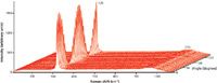
Figure 3: P/O micro-Raman spectra of a (100) face of Si with the light collection analyzer parallel to the incident polarization.
Crystalline samples were put in position on the microscope translation-rotation stage such that the cleaved side of a Si(100) chip was approximately parallel to the incident polarization. We note here that the experimental sample angle is only laboratory bookkeeping and, as we will see later, the crystallographic axis is correlated to the laboratory (or sample packaging) frame through a comparison of the phase of the experimentally obtained P/O plot with that of the corresponding calculated P/O diagram. A plot of the Si(100) parallel polarized Raman spectra as a function of sample orientation (Figure 3) demonstrates that the orientation-dependent relationship of scattering intensity and crystal structure is in good agreement with the calculated response in Figure 1. The first-order Raman band at 520 cm-1 manifests the expected type of sinusoidal variation in signal strength. However, note that the 2TO band between 900 and 1000 cm-1 is invariant with crystal orientation; that is because it arises from second-order Raman scattering. The Raman selection rules are different for first- and second-order Raman scattering, and so the P/O micro-Raman method can be applied to differentiating the two and making band assignments.

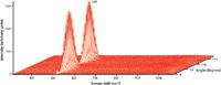
Figure 4: P/O micro-Raman spectra of a (100) face of Si with the light collection analyzer perpendicular to the incident polarization.
The plot of the Si(100) perpendicular polarized Raman spectra in Figure 4 shows the same sinusoidal variation in signal strength and it is 45° out of phase with that of the parallel configuration in Figure 3, consistent with theory. Note the absence of the 2TO band for all orientations and that the signal strength of the 520-cm-1 band is weaker in the perpendicular configuration than in the parallel configuration. That difference in signal strength can be attributed to the different instrument response functions for the two polarizations. Extracting the 520-cm-1 band peak intensities for the two configurations and correcting for the different instrument response functions, the P/O plot of peak areas of the Si(100) 520-cm-1 band is generated and shown in Figure 5.
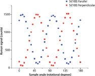
Figure 5: Experimental results for the P/O micro-Raman backscattering experiment with Si(100).
The Si(100) experimental P/O plot consists of two sinusoidal functions 45° out of phase and the plot form is in excellent agreement with the calculated diagram of Figure 1. However, note that calculations predict a maximum response at 0° for the perpendicular configuration, whereas the parallel configuration is near maximum at 0° for the experimentally obtained data. This can be understood in terms of the crystal orientation of the calculation compared to the sample angle with respect to a laboratory reference frame. The approximately 55° phase shift between the experimentally obtained and calculated Si(100) P/O plots is understood as a difference in the crystallographic starting orientations for data collection, and it illustrates an application of P/O micro-Raman spectroscopy for the analysis of texture in natural materials or fabricated devices. P/O plot phase shifts can be used to quantitate the degree of crystallographic orientation or alignment of different features on a micrometer scale relative to a package coordinate system for device fabrication.

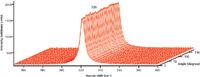
Figure 6: P/O micro-Raman spectra of a (111) face of Si with the light collection analyzer parallel to the incident polarization.
We have found that using the P/O micro-Raman method, crystallographic deviations as small as 2° can be detected, depending on the strength of the Raman signal; that is, the signal-to-noise ratio is generally the limiting factor in this type of crystallographic analysis. To appreciate just how sensitive the P/O micro-Raman method is, consider the orientational invariance of the first-order Raman band at 520 cm-1 obtained from a nominal Si(111) crystal as shown in Figure 6. As you consider the changes in the P/O diagrams as one changes the crystal orientation from (100) to (111), I think that you can begin to appreciate the power of this method.
Conclusions
The theoretical basis for P/O micro-Raman spectroscopy has been discussed, and the feasibility of P/O micro-Raman spectroscopic analysis has been established. P/O micro-Raman spectroscopy may be used to identify vibrational modes, determine crystal structure, distinguish allotropes and polymorphs, differentiate single from polycrystalline materials, and determine orientation of the crystal and degree of disorder, all on a micrometer scale. P/O micro-Raman spectroscopy promises to be an important analytical tool because of its complementarity to micro X-ray diffraction.
David Tuschel is a Raman applications manager at Horiba Scientific, in Edison, New Jersey, where he works with Fran Adar. Starting with this issue, David is sharing authorship of this column with Fran. David can be reached at david.tuschel@horiba.com


David Tuschel
References
(1) F. Adar, Spectroscopy 27(2), 16 (2012).
(2) E.A. Wood, Crystals and Light: An Introduction to Optical Crystallography (D. Van Nostrand, Princeton, New Jersey, 1964).
(3) J.B. Hopkins and L.A. Farrow, J. Appl. Phys. 59, 1103–1110 (1986).
(4) K. Mizoguchi and S. Nakashima, J. Appl. Phys. 65, 2583–2590 (1989).
(5) H.C. Lin, Z.C. Feng, M.S. Chen, Z.X. Shen, I.T. Ferguson, and W. Lu, J. Appl. Phys. 105, 036102 (2009).
(6) M.C. Munisso, W. Zhu, and G. Pezzotti, Phys. Status Solidi B, 246(8), 1893–1900 (2009).
(7) K. Fukatsu, W. Zhu, and G. Pezzotti, Phys. Status Solidi B, 247(2), 278–287 (2010).
(8) W. Hayes and R. Loudon, Scattering of Light by Crystals (John Wiley and Sons, New York, 1978).
(9) G. Turrell, in Raman Sampling. In Practical Raman Spectroscopy, D.J. Gardiner and P.R. Graves, Eds. (Springer-Verlag, New York, 1989), pp 13–54.
(10) E. Bright Wilson, Jr., J.C. Decius, and P.C. Cross, Molecular Vibrations: The Theory of Infrared and Raman Vibrational Spectra. (McGraw-Hill, New York, 1955), p. 285.


Nanometer-Scale Studies Using Tip Enhanced Raman Spectroscopy
February 8th 2013Volker Deckert, the winner of the 2013 Charles Mann Award, is advancing the use of tip enhanced Raman spectroscopy (TERS) to push the lateral resolution of vibrational spectroscopy well below the Abbe limit, to achieve single-molecule sensitivity. Because the tip can be moved with sub-nanometer precision, structural information with unmatched spatial resolution can be achieved without the need of specific labels.


