Raman Spectroscopy of Carbonaceous Materials: A Concise Review
Spectroscopy
A critical review focused on the Raman spectroscopy of carbonaceous materials and of polymer-based nanocomposites that contain carbonaceous (nano) materials as fillers
A critical review focused on the Raman spectroscopy of carbonaceous materials and of polymer-based nanocomposites that contain carbonaceous (nano) materials as fillers is presented. The origin, assignment, and parameters (position, intensity, area, width, and shape) of main Raman modes (radial breathing mode, D-mode, G-mode, G'-mode, and so forth) as well as the effect of the interactions of carbonaceous materials on the parameters of these modes is briefly discussed. The effect of dopants and of polymeric matrices on the parameters of Raman bands is succinctly analyzed. The review will provide the basic and most elementary knowledge required to understand and discuss the Raman spectra of carbonaceous materials.
Carbonaceous materials have a wide range of physical and chemical properties derived from the spatial organization of carbon atoms and their chemical covalent bonds. Diamonds, nanodiamonds, single-walled carbon nanotubes, double-walled carbon nanotubes, carbon nanofibers, and carbon fibers are characterized by an impressive mechanical strength. With the exception of diamond and nanodiamond, the Young modulus of one-dimensional carbonaceous materials decreases as their diameter is increased. This is one of the reasons that nanocomposites based on one-dimensional carbon are extremely attractive. While diamond and nanodiamond are electrical and thermal insulators, one-dimensional carbon nano- and micromaterials, graphene, and graphite are characterized by good electrical and thermal conductivity, exhibiting either semiconducting or conducting features. This wide range of physical properties explains the complex and abundant applications of carbonaceous materials.
Raman spectroscopy investigates the molecular vibrations of atoms and molecules. In a Raman experiment an incoming monochromatic electromagnetic wave (originating from a laser) excites the atoms and molecules of a sample, starting the emittance of electromagnetic radiation. The Raman spectrum is the collection of all these emitted electromagnetic waves, except for the exciting wave (the incident one). This spectrum is generally obtained by using charge-coupled device (CCD) cameras combined with an adequate optics system consisting of prisms or gratings. The position of the Raman spectrum is typically measured in wavenumbers (cm-1) starting from the frequency of the exciting radiation (that has a Raman shift of zero and is not recorded). Most spectrometers start the recording of the Raman spectrum at 50–100 cm-1. The resolution of Raman spectrometers is not critical in the analysis of carbonaceous materials because their lines are not extremely narrow. Typically, Raman spectrometers with a resolution of about 1–3 cm-1 provide excellent research data.
Raman Lines in Carbonaceous Compounds
Several Raman lines (or bands) have been reported in carbonaceous materials and polymer-based nanocomposites containing carbonaceous fillers or nanofillers. The intensity of all these lines depend on the orientation of the polarization relative to the axis of nanotubes (5), the power of the incident laser beam, and the number of accumulations. A typical Raman line for a single-walled carbon nanotubes is shown in Figure 1. The most important Raman lines are discussed in the following sections.

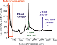
Figure 1: Raman spectrum of single-walled carbon nanotubes.
Radial Breathing Mode
The radial breathing mode (RBM) is related to the diameter of carbon nanotubes and was observed solely in single-walled carbon nanotubes (SWCNT) and double-walled carbon nanotubes (DWCNT) in the range 150–350 cm-1 (7) for diameters of 1–2 nm (8). Typically, RBM is a collective and symmetric movement of all atoms along the radius of the nanotube. In some multiwall carbon nanotubes (MWCNT) and carbon nanofibers (CNF) a broad line can be observed in the region of the RBM, but it is not clear if this line can be actually related to the size diameter of these structures.
The position of the RBM mode in SWCNTs and DWCNTs (ωRBM) depends on the diameter of the nanotube (DT) (8):

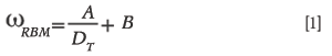
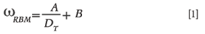
where A and B are constants.
For isolated nanotubes (8), B = 0 and A = 248 nm.cm-1. For bundles of nanotubes, B describes the interactions between nanotubes and is of the order of 10 cm-1, while A = 234 nm.cm-1. For narrow, single-walled carbon nanotubes (DT < 1 nm), the lattice distortions are large, thereby making simple dependencies no longer valid. For SWCNTs with a diameter equal to or larger than 2 nm, the intensity of the RBM mode is too small to be observed (8).
It was reported (4) that the RBM located at 160 cm-1 is broadened and slightly shifted toward higher positions (ω) as the isolated nanotubes collapse into a bundle. For an isolated SWCNT, the width of the RBM mode is of the order of 3 cm-1.
The RBM has also been reported in fullerenes, typically below 250 cm-1 although it also was reported at 490 cm-1 (11). The position of the RBM mode in fullerenes depends on the energy (wavelength) of the incoming laser beam (12).


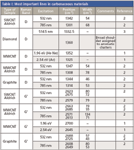
Table I: Most important lines in carbonaceous materials
D-Band
The disorder- or distortion-band (D-band) is typically located between 1300 and 1450 cm-1, originates from sp3 carbon, and is strongly influenced by the amount of carbon impurities present. The D-band is highly dispersive, and its position is dependent on the wavelength of the incident laser beam. With an acceptable accuracy, the position of the D-band depends linearly on the energy (wavelength) of the incoming laser beam (7). The position of the D-band in diamond crystals is affected by local stresses σ (in GPa) (3):

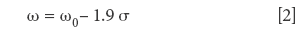

where ω0 = 1332 cm-1.
G-Band
The graphite-band (G-band) is a first-order Raman process located between 1500 and 1600 cm-1 and is assigned to graphitic structures. Typically, the G-band is not dispersive; for instance, the position of this band is not affected by the wavelength of the incoming laser beam (4). The G-band is usually associated with sp2 structures (1,2,4). The G+ component was observed in insulating carbon nanotubes (4,5). This line is narrow, has a typical Lorentzian shape, and corresponds to vibrations along the direction of the nanotube; its position is not affected by the diameter of carbon nanotubes. The G-component was noticed at smaller Raman frequencies and corresponds to circumferential vibrations (5). The G-line is broader than the G+ line and deviates from the Lorentzian shape (this typically has a Breit-Wigner-Fano [BWF] shape [5]). This component has been reported (4,5) in semiconducting and conducting nanotubes and depends on the diameter of the nanotubes (the Raman frequency of the G-component increases as the diameter of nanotube is increased [3]).
The position of the G-line, ωG- is related to the diameter on nanotubes, D through


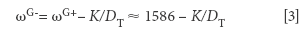
where K = 47.7 nm.cm-1 for semiconducting nanotubes and K = 79.5 nm.cm-1 for conducting nanotubes (5). The advantage of this expression derives from the fact that ωG+ does not depend on the wavelength of the incoming laser beam.
G'-Band
The G'-band (or the D*-band (7) or the 2D band [14]) is an overtone (2 phonon process) of the D-band located between 2450–2950 cm-1. Both the D- and G'-bands exhibit a more pronounced dependence of the Raman line position on the energy (frequency) of the incoming electromagnetic radiation compared to the G-band (1). The G'-band is related to the presence of sp2 (graphitic) bonds (13). This shift (expressed as dω/dEL where ω defines the position of the G'-band in cm-1 and EL defines the energy of the incoming laser beam (which can exceed 100 cm-1 /eV [4]). An acceptable equation for the G'-band position is

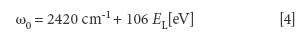

It is speculated that the ratio between the (integrate) intensity of the G'-band and the (integrated) intensity of the D-band is more sensitive to the purity of MWCNTs and less affected by the energy (frequency) of the incoming electromagnetic radiation. The G'-line in graphene depends on the number of graphene layers (13,14).
Additional Lines
In irradiated graphene a new line located at about 1625 cm-1 was noticed (labeled D') and associated with local disorder (13). There also was a report in graphene (6) that there was a strong G + D line located at 2940 cm-1 and a G*-line at 2450 cm-1 (15). The G*-line also is a dispersive line, but the position of the Raman peak shifts toward a smaller Raman shift (in cm-1) as the energy (frequency) of the incident laser beam is increased (for the G'-line the Raman peak shifts towards a larger Raman shift as the energy of the incident laser beam is increased) (15).
An additional line (named T-line) has been reported in amorphous carbons when the incoming laser beam is in the UV range (17) and assigned to sp3 carbons. In hydrogenated amorphous carbons this shift is shifted up to 980 cm-1. This line should not be confused with the tangential mode, sometimes labeled as T-mode.
Raman Lineshape
A general expression for the Raman lineshape can be written as follows

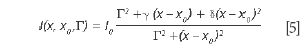

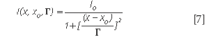
Equation 5 degenerates into a BWF lineshape if δ= ε2 and γ= 2εΓ = 2 Γδ1/2:


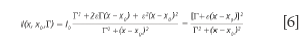
For BWF lineshapes, the parameter ε is typically replaced with 1/q. The advantage of this notation comes from the immediate identification of the physical significance of the parameters δ or ε, that describe the deviation of the lineshape from the simple symmetrical Lorentzian lineshape.
The situation in which ε is very small, hence, the term in ε2 can be neglected, was briefly discussed (10). Assuming γ= δ= 0, the generalized expression of the lineshape degenerates into a classical symmetric Lorentz lineshape. Equation 5 shows that the parameter γ is associated with an asymmetric distortion of the Lorentz lineshape and the parameter δ corresponds to a symmetrical distortion of the Lorentz lineshape. The parameter δ measures the interaction of phonons with a continuum of states and was found to be negative in metallic single-walled carbon nanotubes.


The Raman linewidth can be expressed as (12)

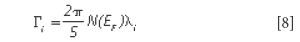

where N(EF) is the density of the electrons at the Fermi level and λ is the electron-phonon coupling constant for the mode "i" (12).
Facts and Artifacts in Raman Spectroscopy
Typically, the degree of disorder is measured by the ratio of the D- (some authors prefer D') and G-bands. There are two possible ratios: The first one is the ratio of the amplitude of the Raman lines, labeled as ID/IG (or ID'/IG) and the second is the ratio between the integral or integrated amplitude AD/AG (or AD'/AG). The integral (or integrated) intensity is actually the area of the Raman peak and contains both the contribution of the line amplitude and width. From the spectroscopic point of view, the number of carbon atoms contributing to the D-, D'-, or G-lines is proportional to the area of the recorded line and not to its intensity. Hence, all data that are using ID/IG (or ID'/IG) should be considered with caution. We suggest using the notation AD/AG (or AD'/AG) to specify that the ratio refers to the areas of the peaks.
Another source of error originates from using high densities (the ratio between the laser power and the exposed area) of incoming light. Under such circumstances, the sample is heated by the incoming laser beam and the parameters of the Raman spectrum are modified. Although it is difficult to specify a limit for the ratio between the power of the laser beam and the area exposed to the beam for all materials, a simple rule of thumb might be sufficient for accurate answers. This means the successive recording of three Raman spectra. If all three are identical, then the sample's heating is negligible and the data, as obtained, are solid.
While the position of G', D*, or 2D is almost twice the position of the D-band, the terminology 2D-band or D*-band is misleading because the line was observed even in the absence of defects (15).
To have reliable data in a confocal Raman microscope, it is mandatory to focus on the sample and if possible to check that at the end of the measurement the image of the sample is still focused.
Raman Lines in Carbonaceous Materials and Polymer-Based Nanocomposites with Carbonaceous Fillers
In the case of carbon nanoclusters, it was reported that the thermal annealing in the temperature range 200–800 °C ignites a graphitization process that enhances the degree of disorder, narrows the D- and G-lines, decreases the energy gap, and is responsible for a weak blue shift of the G-line as the annealing temperature is increased (9). A linear dependence of the position of the G'-line on temperature has been reported in graphene (14). The oxidation of graphene converts the almost symmetric D- and G-Raman bands into strongly asymmetric spectra (16).
In graphite, the 2D peak is a superposition of two peaks 2D1 and 2D2 (17). Typically, the Raman lines of carbonaceous materials dispersed in polymeric materials are dominating over the spectrum of the polymeric matrix, for concentrations of carbonaceous materials in excess of 5 % (wt) (18). The dispersion of carbon nanofibers within isotactic polypropylene shifts the position of the D- and G-lines, moving them toward a larger value as the concentration of carbon nanofibers is increased up to 15 % (wt) and broadens them (18). As expected, the degree of disorder is enhanced by increasing the amount of carbon nanofibers in the polymeric matrix. Ionizing radiation changes the distribution of the diameters of single-wall carbon nanotubes and enhances the disorder within them (19). Complex changes were reported in chemically modified carbon nanostructures (20).
Conclusions
Raman spectroscopy is extremely sensitive to the presence of carbonaceous materials. Specific line parameters (position, width, shape, and relative integral amplitude) can provide additional information about dopants, physical and chemical modification of the surface, and the effect on the dispersion of such materials within polymers. The Raman spectrum is usually dominated by sp2 bonds, interactions, and clustering, as well as the disorder introduced within carbonaceous materials, the presence of sp2 cyclic structures, the sp2/sp3 ratio, and the presence of sp structures. However, Raman alone cannot always be used to uniquely assign a spectrum to a given carbonaceous material. Raman lines are sensitive to temperature, pressure, and stress or strain. Physical and chemical modifications including doping and grafting of new chemical residues affect the parameters of Raman lines because of local modifications of symmetry. Dispersion of carbonaceous materials within polymers showed changes in the parameters associated to Raman lines of the fillers.
Dorina Magdalena Chipara, and Mircea Chipara are with the University of Texas-Pan American, Department of Physics and Geology, Edinburg, Texas. Please direct correspondence to: chipara@yahoo.com.
Alin Cristian Chipara is with the University of Texas-Pan American, Department of Mechanical Engineering, Edinburg, Texas.
References
(1) R. DiLeo, B. Landi, and R. Raffaelle, Mater. Res. Soc. Symp. Proc. 1018, 1018–EE05-11 (2007).
(2) H.M. Heise, R. Kuckuk, A.K. Ojha, A. Srivastava, V. Srivastava, and B.P. Asthana, J. Raman Spectrosc. 40, 344–353 (2009).
(3) S. Gupta, O. Williams, R.J. Patel, E. Bohannan, and P.W. May, Mater. Res. Soc. Symp. Proc. 977, 0977–FF04-18 (2007).
(4) M.S. Dresselhaus, A. Jorio, A.G. Souza Filho, G. Dresselhaus, R. Saito, and M.A. Pimenta, Mat. Res. Soc. Symp. Proc. 706, Z.7.1.1.–Z.7.1.11 (2002).
(5) M.S. Dresselhaus, G. Dresselhaus, A. Jorio, A.G. Souza Filho, and R. Saito, Carbon 40, 2043–2061 (2002).
(6) R.K. Paul, S. Badhulika, S. Niyogi, R.C. Haddon, V.M. Boddu, C. Costales-Nieves, K.N. Bozhilov, and A. Mulchandani, Carbon D-11-00661 49, 3789–3795 (2011).
(7) Q. Zhao and H.D. Wagner, Phil. Trans. R. Soc. Lond. A 362, 2407–2424 (2004).
(8) A. Jorio, M.A. Pimenta, A.G. Souza Filho, R. Saito, G. Dresselhaus, and M.S. Dresselhaus, New J. of Phys. 5, 139.1–139.17 (2003).
(9) G. Compagnini, O. Puglisi, and M. Chipara, Mater. Res. Soc. Symp. Proc. 887, 0887–Q01-03.1 (2006).
(10) A.C. Chipara, T. Mion, R. Villegas, K. Lozano, M.D. Chipara, S. Tidrow, and M. Chipara, Mater. Res. Soc. Symp. Proc. 1204, 1204–K10-15 (2010).
(11) U.D. Venkateswaran, A.M. Rao, E. Richter, M. Menon, A. Rinzler, R.E. Smalley, and P.C. Eklund, Phys. Rev. B 59(16), 10928–10934 (1999).
(12) H. Kuzmany, R. Pfeiffer, M. Hulman, and C. Kramberger, Phil. Trans. R. Soc. Lond. A 362, 2375–2406 (2004).
(13) M.S. Dresselhaus, A. Jorio, M. Hofmann, G. Dresselhaus, and R. Saito, Nano Lett. 10, 751–758 (2010).
(14) I. Calizo, A.A. Balandin, W. Bao, F. Miao, and C.N. Lau, Nano Lett. 7(9), 2645–2649 (2007).
(15) L.M. Malard, M.A. Pimenta, G. Dresselhaus, and M.S. Dresselhaus, Phys. Rep. 473, 51–87 (2009).
(16) K.N. Kudin, B. Ozbas, H.C. Schniepp, R.K. Prud'homme, I.A. Aksay, and R. Car, Nano Lett. 8(1), 36–41 (2008).
(17) A.C. Ferrari, Sol. St. Commun. 143, 47–57 (2007).
(18) M. Chipara, J.R. Villarreal, M.D. Chipara, K. Lozano, A.C. Chipara, and D.J. Sellmyer, J. of Poly. Sci.: Part B: Poly.Phys. 47, 1644–1652 (2009).
(19) A.R. Adhikari, M. Huang, H. Bakhru, M. Chipara, C.Y. Ryu, and P.M. Ajayan, Nanotech. 17, 5947–5953 (2006).
(20) C.T. Ramos, R. Thapa, K. Lozano, M. Chipara, D. Ferrer, and J.J. Gutierrez, J. of Nanosci. and Nanotech. 11, 3965–3969 (2011).


Nanometer-Scale Studies Using Tip Enhanced Raman Spectroscopy
February 8th 2013Volker Deckert, the winner of the 2013 Charles Mann Award, is advancing the use of tip enhanced Raman spectroscopy (TERS) to push the lateral resolution of vibrational spectroscopy well below the Abbe limit, to achieve single-molecule sensitivity. Because the tip can be moved with sub-nanometer precision, structural information with unmatched spatial resolution can be achieved without the need of specific labels.


