Three-Dimensional Raman Imaging of Ion-Exchanged Waveguides
Segmented channel waveguides have been fabricated in single-crystal KTiOPO4 through a topotactic process of partial cation exchange. The ion-exchanged waveguides maintain the high nonlinear susceptibility of KTiOPO4 to function as frequency doubling laser light sources
Segmented channel waveguides have been fabricated in single-crystal KTiOPO4 through a topotactic process of partial cation exchange. The ion-exchanged waveguides maintain the high nonlinear susceptibility of KTiOPO4 to function as frequency doubling laser light sources. We applied three-dimensional Raman imaging to understand and characterize the changes to the chemical bonding and crystalline structure as well as measure the volumetric structure of the waveguide segments.
The ion-exchange process is a convenient method for the fabrication of channel waveguides in crystals with high nonlinear susceptibility and electro-optic coefficients. The idea is to create a channel in which the refractive index has been sufficiently changed to achieve laser beam confinement (wave guiding) while retaining the high nonlinear optical susceptibility of the host crystal. Through either quasi-phase matching in continuous waveguides or balanced phase matching in segmented waveguides, second harmonic generation can be achieved to produce short-wavelength laser output from an end-fired near-infrared laser beam. The waveguides are generated through a topotactic chemical reaction in which a nonlinear single crystal of LiNbO3 or KTiOPO4 is exposed to an acid or salt melt with a cation different from that of the host crystal. For example, if a single crystal of KTiOPO4 is exposed to RbNO3 at an elevated temperature over a select period of time, a cation exchange will occur forming RbxK1-xTiOPO4 in a certain volume near the surface of the crystal. For those interested in this type of chemical reaction, I described the process of topotactic chemistry by H+ ion exchange in LiNbO3 in a previous installment of "Molecular Spectroscopy Workbench" (1). Waveguides fabricated in this fashion have a technological function as frequency doubled waveguide lasers, electro-optic shifters, and Mach-Zehnder interferometric devices. This is the world of integrated optics and electro-optics. The goal in ion-exchange waveguide fabrication is to sufficiently change the refractive index of the host crystal to achieve confinement of the laser light beam incident upon the end face of the device without significantly altering the electro-optic properties or nonlinear susceptibilities of the waveguide relative to those of the host crystal. Furthermore, this must be done to create a patterned three-dimensional (3D) volume of optical circuitry. To understand and control these fabrication processes as well as the final performance of the device, a method of 3D imaging of the chemical bonding, solid state structure, and volumetric structure is essential. Here, we discuss the 3D Raman imaging of Rb+-exchanged KTiOPO4 segmented channel waveguides.
The waveguides are fabricated by depositing a metal coating on the Z-face of the crystal and subsequently using photolithographic techniques to create a pattern of openings in the metal. The open areas are exposed for ion exchange to form the waveguides and optical circuitry. A typical process exposes the KTiOPO4 surface to RbNO3 at elevated temperatures; for example, 350 °C for 20 min (2). The temperature and particularly the duration of the ion-exchange process affect the final volumetric structure of the waveguides. We show that Raman imaging of KTiOPO4 exposed to RbNO3 for different durations reveals the effect of the ion-exchange process on the final volumetric structure of the waveguides.

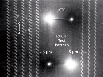

Figure 1: Cross-polarized transmitted white light image of Rb+-exchanged KTiOPO4 waveguides and test pattern. Incident white light is polarized along the crystallographic x-axis with the analyzer oriented along the crystallographic y-axis.
A cross-polarized image of a Rb+-exchanged KTiOPO4 device is shown in Figure 1. The transmitted white light was polarized parallel to the crystallographic x-axis of the KTiOPO4 and the analyzer was oriented parallel to the crystallographic y-axis. Under such conditions of cross-polarization one should observe no transmitted light; however, the regions subjected to Rb+ ion exchange do transmit light, thereby indicating a local distortion of the KTiOPO4 crystallographic axes. A second image of the waveguides acquired at a higher magnification, but under the same cross-polarization conditions is shown in Figure 2. These waveguides were fabricated to produce blue to green laser light through frequency doubling of a near-infrared diode laser end-fired into the end Y-face of the segmented waveguide. (By definition, the Y-face is that face which is perpendicular to the y-axis. Of course, the same applies for the X- and Z faces.) These particular waveguides are segmented to achieve balanced phase matching, a technique shown to yield phase matching and highly efficient second harmonic conversion (3). Here, you can clearly see the structure of the waveguides consisting of intermittent segments of Rb-exchanged KTiOPO4 (RbxK1-xTiOPO4) and the native KTiOPO4. The segmented waveguides travel along the y-axis. The brightness, and therefore birefringence, of the waveguide end segments reveal far more distortion to chemical bonding and crystal structure from the Rb+-exchange at the end segments than to all of the Rb+-exchanged segments in the crystal interior.

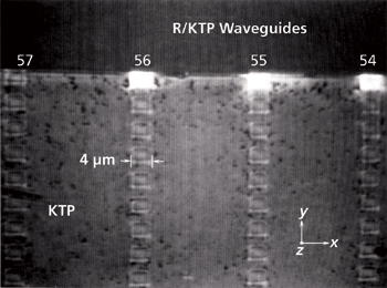
Figure 2: Cross-polarized transmitted white light image of Rb+-exchanged KTiOPO4 waveguides and test pattern. Incident white light is polarized along the crystallographic x-axis with the analyzer oriented along the crystallographic y-axis.
Raman Spectroscopy of Rb-Exchanged KTiOPO4
To understand the spectral changes observed in the Rb+-exchanged regions of KTiOPO4 (R/KTP) we need to first consider the Raman spectra of single crystals of KTiOPO4 (KTP) and RbTiOPO4 (RTP). The spectra of the single crystals and the ion-exchanged waveguides are highly dependent on the crystal orientation relative to the direction of the incident laser beam and polarization. It happens that the most dramatic Raman spectral differences among KTP, RTP, and R/KTP are observed when focusing the incident laser beam on the crystalline Y-face with light polarized along the z-axis viewing the end face of the device. However, the acquisition of 3D Raman images along the waveguides requires viewing the top of the device (the Z-face), and so we will restrict our comparison of single-crystal spectra to those obtained with the beam incident on the Z-face. Raman spectra of single crystals of KTiOPO4 and RbTiOPO4 are shown in Figure 3. The inset Porto notation indicates that the laser beam propagated along the z-axis incident upon the Z-face of the crystal with polarization along the y-axis and backscattered light was collected without the use of a polarization analyzer (YX). The KTiOPO4 and RbTiOPO4 spectra are similar because the Raman scattering from both crystals arises primarily from the octahedral TiO6 and tetrahedral PO4 structural units. The greater differences appear at Raman shifts less than 375 cm-1 where the neighboring cation has a more significant effect on the vibrational bending motions of the TiO6 and PO4 groups.

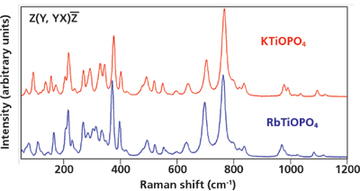
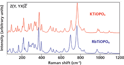
Figure 3: Raman spectra of KTiOPO4 and RbTiOPO4 single crystals.
These KTiOPO4 and RbTiOPO4 spectra would normally represent our spectral limits as we analyze compounds with varying stoichiometries of K1-xRbxTiOPO4 prepared from a melt. However, remember that our waveguides are prepared by a topotactic chemical reaction in which the host crystal, which is built for the K+ ion, exchanges some of the cations for the Rb+ ion. Therefore, we have an entirely different structure than one that would be formed from a mixed stoichiometric composition generated from the melt in which the most energetically favorable bond lengths, bond angles, and lattice spacings would be established for the specific K1-xRbxTiOPO4 composition. Here you have the Rb+ ion with a much larger atomic radius (r = 1.49 Å) replacing K+ (r = 1.33 Å) in a crystal "built" for the smaller K+ cation. You can appreciate the importance of this difference by viewing the Ti coordination environment of KTiOPO4 shown in Figure 4. The exchange of K+ for Rb+ increases the chemical interaction of the TiO6 species with the larger Rb+ cation, induces strain in the crystal lattice, and forces a change in the solid state structure to reduce the energy. These changes in chemical bonding and solid-state structure are the origin of the local change in the refractive index to form a waveguide and the birefringence seen in Figures 1 and 2.

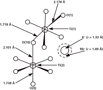
Figure 4: Ti coordination environment in KTiOPO4.
The most dramatic Raman spectral changes in R/KTP can be detected by probing the waveguide end Y-face with Z-polarized light. However, we wish to generate 3D Raman images along the waveguide; therefore, we need to map the Z-face with the incident laser beam parallel to the z-axis. Raman spectra of a region of R/KTP and KTP adjacent to it are shown in Figure 5. These spectra are plotted in absolute counts and are not normalized. The Raman band at 637 cm-1 is significant insofar as it has the same signal strength for R/KTP and the adjacent KTP. Therefore, any differences in the absolute strengths of the other bands indicate varying differences in relative strengths between R/KTP and KTP Raman bands, thereby allowing an easy distinction of the two compositions. In particular, note the reversal in 270 and 293 cm-1 relative band strength in transforming KTP to R/KTP. Consequently, the application of direct classical least squares analysis to the hyperspectral data set acquired by mapping in either two dimensions (2D) or 3D produces Raman images of the waveguides and host crystal based on their distinct Raman signatures arising from changes in chemical bonding and solid-state structure. All Raman images shown here were generated by direct classical least squares analyses in supervised mode; that is, target image spectra were fit with acquired reference spectra of KTP and R/KTP.

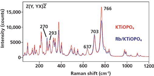
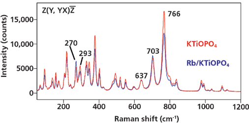
Figure 5: Raman spectra of a Rb+-exchanged KTiOPO4 region and the KTiOPO4 adjacent to it.
A 2D Raman image of the end portion of one of the waveguides is shown in Figure 6a. This particular waveguide is from the same optical device shown in Figures 1 and 2. The data were acquired using a 100× objective, 532-nm excitation, and controlled movement of an electronic stage in 0.2-µm x and y spatial increments. The application of a direct classical least squares treatment of the hyperspectral data is the basis for the image in which red corresponds to KTP and black to R/KTP. Note the smearing in the Raman image at the top segment of the waveguide and how well it comports with the strain birefringence of the top segments seen in Figure 2, particularly waveguide number 55. Also, one can see the same kind of spotted KTP defects in the Raman image that are observed in Figure 2 by cross-polarized transmitted light microscopy. Figure 6b shows a 2D Raman image obtained from an entirely different R/KTP waveguide device prepared with different segment dimensions, in particular a narrower KTP gap between the R/KTP segments. This device was also mapped in 0.2-µm x and y spatial increments using a 100× objective and 532-nm excitation. Note the clarity of the image and the registration over a length exceeding 60 µm. Tight stage motion and positioning are absolutely critical for such high-resolution Raman imaging, and that is particularly true when extending 2D area maps to the third dimension.

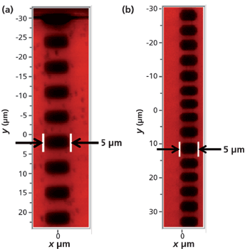
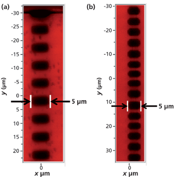
Figure 6: Raman images of waveguides from (a) the same device shown in Figures 1 and 2, and (b) another device with narrower spacings between the R/KTP segments.
3D Raman Imaging of Segmented Waveguides
We applied 3D Raman imaging to understand and characterize changes to the chemical bonding and solid-state structure as well as to measure the volumetric structure of the waveguide segments. A 3D Raman image of a portion of a segmented waveguide is shown in Figure 7. The hyperspectral data that form the basis of the image were acquired in 0.2-µm xy increments with axial spacings of 2 µm from the surface to a final translation stage position of -10 µm. The dimensions that appear on the box framing the image in Figure 7 (and all subsequent volumetric Raman images) correspond to the dimensions of the full image within the box. Thus, you see a segmented channel waveguide imaged over 42.7 µm (y-axis) by 12.6 µm (x-axis) over a stage travel depth of 10 µm. We note here that the depth dimensions reported and shown in the images are actually of axial stage position only. The axial stage positions do not correspond precisely to the actual focal depth of the laser beam in the material. To obtain truly quantitative confocal images, one must take into account the effect of the material's refractive index on the laser beam focus. To do that, we refer readers to the indispensable work on this subject by Neil Everall (4–8).


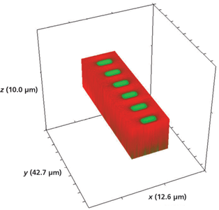
Figure 7: 3D Raman image of a portion of a segmented Rb+-exchanged KTiOPO4 waveguide device fabricated by exposing open surfaces to molten RbNO3 for 20 min.

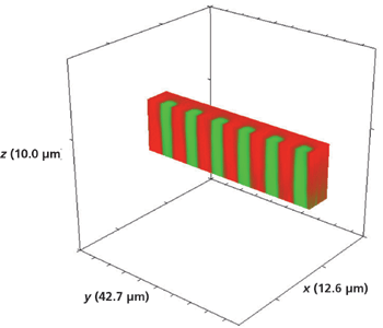
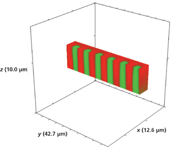
Figure 8: Sliced portion of the 3D Raman image of the waveguide shown in Figure 7.
Three-dimensional Raman imaging is best suited for a real-time display during which one can slice through the voxels to uncover the planar images hidden within that reveal spatially varying changes in chemical composition, bonding, and solid-state structure. Since we are restricted to the presentation in print form, we opted for showing a volumetric image with a portion sliced away to reveal the structure within. Figure 8 shows the volumetric image of Figure 7 with approximately one-half of the x-axis portion of the original 3D image sliced off to expose the depth of the Rb+-exchanged waveguide segments. The most striking aspect revealed by the 3D imaging is how the exchange occurs so deeply and uniformly along the crystallographic z-axis. There is almost no lateral mass transport of Rb+. This is quite contrary to the radial diffusion that one might have expected, similar to that observed when placing a drop of a colored fluid in another that is transparent. Furthermore, we can see in this image the degree of Rb+ exchange is beginning to diminish only near a depth of 10 µm. To get a more detailed image of the Rb+ exchange process in lateral and axial dimensions, we obtained a 3D image of the corner of the R/KTP test pattern seen in Figure 1. A Raman hyperspectral data set was acquired by translating the sample in 0.2-µm x and y increments and 0.5-µm increments along the z-axis. The 3D image of the full volume x (11.2 µm), y (7.6 µm), and z (14.0 µm) is shown in Figure 9. The Rb+ exchange is somewhat irregular at the greatest depth along the z-axis and ends at a depth of approximately 10 µm. The sharp and vertical axial borders to the Rb+-exchanged R/KTP test pattern are really quite remarkable, showing little evidence of lateral mass transport and Rb+ exchange in the direction along the xy-plane.

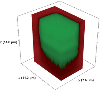
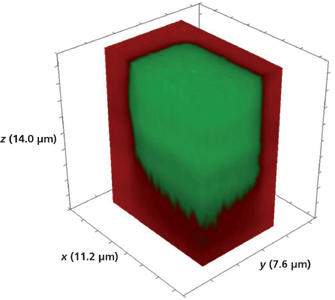
Figure 9: 3D Raman image of a portion of a R/KTP test pattern of a Rb+-exchanged KTiOPO4 waveguide device fabricated by exposing open surfaces to molten RbNO3 for 20 min.

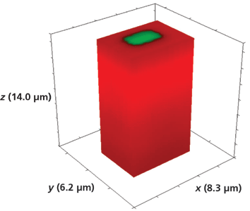
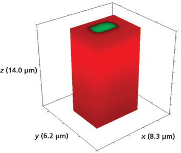
Figure 10: 3D Raman image of one segment of a Rb+-exchanged KTiOPO4 waveguide exposed to molten RbNO3 for 20 min.
Turning now to a deeper analysis of the segmented waveguides, the 3D image of the full volume x (8.3 µm), y (6.2 µm), and z (14.0 µm) Rb+-exchanged segment is shown in Figure 10. The Raman hyperspectral data set was acquired by translating the sample in 0.2-µm x and y increments and 1.0-µm increments along the z-axis. This is a 5-µm-wide Rb+-exchanged segment, and over a depth of 14 µm there is no indication of lateral transport of the Rb+ ions in the xy-plane to the borders or outer surfaces of the 3D image. Rotating the full volumetric image, adjusting the transparency of the two components, and slicing off planes of the volumetric data set is the ideal way of analyzing a 3D Raman image. However, as we already stated, we are restricted to the print page so a look at volumetric fractions will have to suffice. Figure 11 shows the same volumetric data set but with one-half of the y-axis sliced off to reveal the 3D structure of one 5-µm Rb+-exchanged segment. We see that the axial boundaries are indeed vertical with the Rb+ exchange tapering off at a depth of approximately 10 µm.

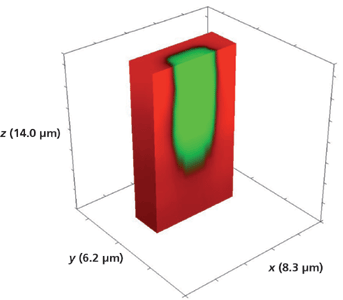

Figure 11: Sliced portion of the 3D Raman image of one segment of a Rb+-exchanged KTiOPO4 exposed to molten RbNO3 for 20 min shown in Figure 10.

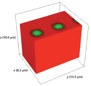
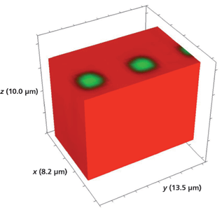
Figure 12: 3D Raman image of a portion of a segmented Rb+-exchanged KTiOPO4 waveguide exposed to molten RbNO3 for 20 min.
A reasonable question: Would a smaller size of the opening in the metal mask affect the lateral mass transport and therefore the depth aspect ratio of the waveguide segments? We have seen that both the large R/KTP test pattern and the 5-µm R/KTP segment have depths of approximately 10 µm. The smallest segment width of the waveguide device shown in Figure 1 is 3 µm. A Raman hyperspectral data set of the 3-µm Rb+-exchanged segmented waveguide was acquired by translating the sample in 0.5-µm x and y increments and 1.0-µm increments along the z-axis. The 3D image of the full volume x (8.2 µm), y (13.5 µm), and z (10.0 µm) is shown in Figure 12. Again, we see no evidence of lateral mass transport of Rb+ exchange over a depth of 10 µm to the outer border or surface of the full volumetric image. Slicing away a portion of the x-axis and the y-axis exposes the volumetric structure of the waveguide segments as shown in Figures 13 and 14, respectively. Even for the small 3-µm Rb+ exchanged segments the mass transport occurs strictly along the crystallographic z-axis with no evidence of lateral mass transport of Rb+ exchange in the crystallographic xy-plane.


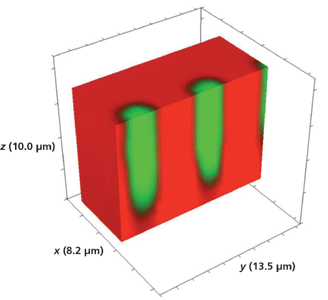
Figure 13: Sliced portion of the 3D Raman image of a segmented Rb+-exchanged KTiOPO4 waveguide exposed to molten RbNO3 for 20 min shown in Figure 12.
The important conclusion from these Raman images with respect to the fabrication of Rb+-exchanged KTiOPO4 waveguides is that the pattern and sizes of the openings in the mask on the crystal face will be retained axially as the mass transport of Rb+ exchange occurs almost exclusively along the crystallographic z-axis of KTiOPO4.

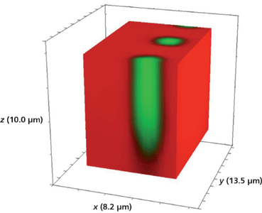
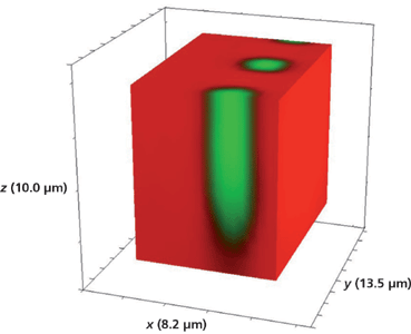
Figure 14: Sliced portion of the 3D Raman image of a segmented Rb+-exchanged KTiOPO4 waveguide exposed to molten RbNO3 for 20 min shown in Figure 12.
Controlling Waveguide Depth
We have seen that segmented waveguides and even large area test patterns fabricated by Rb+ exchange all have comparable depths for which the mass transport of Rb+ exchange is almost exclusively along the crystallographic z-axis of KTiOPO4. Experiments have confirmed that the temperature of the molten RbNO3 and, far more importantly, the duration of its exposure to the crystal through the openings in the mask deposited on the Z-face determine the final depth of the waveguides. In this final section, we examine Raman images obtained from devices fabricated by exposure to RbNO3 at approximately 380 °C, but for a fraction of the time for the devices shown in Figures 1 and 2. The device that we now examine has been exposed to molten RbNO3 for 10 min, which is one-half the exposure time for the waveguide devices discussed earlier. Figure 15 shows a 3D Raman image of the full volume x (8.3 µm), y (6.2 µm), and z (14.0 µm) surrounding a 5-µm Rb+-exchanged segment. The hyperspectral data set was acquired by translating the sample in 0.2-µm x and y increments and 1.0-µm increments along the z-axis. We see no evidence of lateral mass transport of Rb+ exchange over a depth of 14 µm to the outer border or surface of the full volumetric image. Slicing away a portion of the y-axis exposes the volumetric structure of the waveguide segment as seen in Figure 16. Here, we see that the depth of the segment is 5 µm, one-half the depth observed for the waveguide exposed for 20 min. So, it appears that the depth of the waveguide segment is proportional to the duration of exposure to the RbNO3 melt.

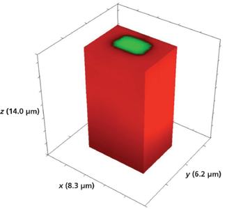

Figure 15: 3D Raman image of one segment of a Rb+-exchanged KTiOPO4 waveguide exposed to molten RbNO3 for 10 min.

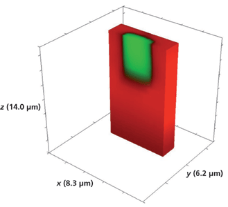
Figure 16: Sliced portion of the 3D Raman image of one segment of a Rb+-exchanged KTiOPO4 waveguide exposed to molten RbNO3 for 10 min shown in Figure 15.
Another device that we examined had been exposed to molten RbNO3 for 5 min. Figure 17 shows a 3D Raman image of the full volume x (8.2 µm), y (27.2 µm), and z (15.0 µm) surrounding a series of 3 µm Rb+-exchanged segments. The hyperspectral data set was acquired by translating the sample in 0.5-µm x and y increments and 1.0-µm increments along the z-axis. Again, there is no evidence of lateral mass transport of Rb+ over a depth of 14 µm to the outer border or surface of the full volumetric image. Slicing away a portion of the x-axis and the y-axis exposes the volumetric structure of the waveguide segments as seen in Figures 18 and 19, respectively. Here, we see that the depth of the segment is 3 µm, approximately one-half the depth observed for the waveguide exposed for 10 min.
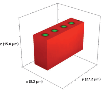
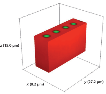
Figure 17: 3D Raman image of a portion of a segmented Rb+-exchanged KTiOPO4 waveguide exposed to molten RbNO3 for 5 min.
The conclusion that we can draw from the 3D Raman imaging of Rb+-exchanged KTiOPO4 waveguides is that the depth of the waveguide segment is linearly proportional to the duration of exposure to the molten RbNO3 and that the time of Rb+ exchange has no effect on the lateral mass transport of Rb+ exchange and depth aspect ratio of the Rb+-exchanged segments.

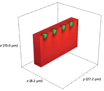
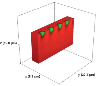
Figure 18: Sliced portion of the 3D Raman image of a portion of a segmented Rb+-exchanged KTiOPO4 waveguide exposed to molten RbNO3 for 5 min shown in Figure 17.
Conclusions
We applied 3D Raman imaging to understand and characterize the changes to the chemical bonding and crystalline structure as well as measure the volumetric structure of the waveguides formed through topotactic chemical reactions. Raman images of Rb+-exchanged KTiOPO4 waveguides reveal that the pattern and sizes of the openings in the mask created by photolithographic processes on the crystal Z-face will be retained axially as mass transport of Rb+ exchange occurs almost exclusively along the crystallographic z-axis of KTiOPO4. The depth of the waveguide segment is linearly proportional to the duration of exposure to the molten RbNO3 and that the time of Rb+ exchange has no effect on the lateral mass transport of Rb+ exchange and depth aspect ratio of the Rb+-exchanged segments.
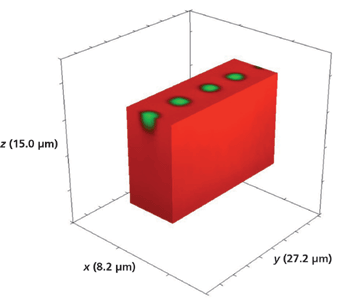

Figure 19: Sliced portion of the 3D Raman image of a portion of a segmented Rb+-exchanged KTiOPO4 waveguide exposed to molten RbNO3 for 5 min shown in Figure 17.
References
(1) D. Tuschel, Spectroscopy27(9), 14–19 (2012).
(2) D.D. Tuschel, G.R. Paz-Pujalt, and W.P. Risk, Appl. Phys. Lett.66, 1035–1037 (1995).
(3) J.D. Bierlein, D.B. Laubacher, J.B. Brown, and C.J. van der Poel, Appl. Phys. Lett.56, 1725–1727 (1990).
(4) N.J. Everall, Appl. Spec.54, 773–782 (2000).
(5) N.J. Everall, Appl. Spec.54, 1515–1520 (2000).
(6) N.J. Everall, J. Raman Spec.45, 133–138 (2014).
(7) N.J. Everall, Spectroscopy19(10), 22–27 (2004).
(8) N.J. Everall, Spectroscopy19(11), 16–25 (2004).
David Tuschel is a Raman applications manager at Horiba Scientific, in Edison, New Jersey, where he works with Fran Adar. David is sharing authorship of this column with Fran. He can be reached at: david.tuschel@horiba.com.


David Tuschel


Nanometer-Scale Studies Using Tip Enhanced Raman Spectroscopy
February 8th 2013Volker Deckert, the winner of the 2013 Charles Mann Award, is advancing the use of tip enhanced Raman spectroscopy (TERS) to push the lateral resolution of vibrational spectroscopy well below the Abbe limit, to achieve single-molecule sensitivity. Because the tip can be moved with sub-nanometer precision, structural information with unmatched spatial resolution can be achieved without the need of specific labels.


