A Comparison of Raman Analysis of Carbon Nanotubes
Application Notebook
A new Raman spectrometer system, innoRamâ„¢, has been developed to provide research-grade performance in either a lab or a mobile environment. The Raman analysis of carbon nanotubes using innoRam in comparison with a Raman spectrometer using a conventional front illuminated CCD demonstrates distinctive improvements for innoRam in both sensitivity and signal-to-noise ratio (SNR).
Dawn Yang, B&W Tek, Inc.
A new Raman spectrometer system, innoRam™, has been developed to provide research-grade performance in either a lab or a mobile environment. The Raman analysis of carbon nanotubes using innoRam in comparison with a Raman spectrometer using a conventional front illuminated CCD demonstrates distinctive improvements for innoRam in both sensitivity and signal-to-noise ratio (SNR).
B&W Tek's newly developed Raman system, innoRam™, is a research-grade Raman spectrometer with high sensitivity and application versatility. The innoRam's back-thinned 2D vertically binned CCD detector with TE-cooling to –20 °C ensures research-grade performance. The application discussed in this paper is a comparison of Raman analysis of carbon nanotubes between innoRam and a Raman spectrometer with front-illuminated linear CCD detector with TE-cooling to 14 °C.
Compared with a conventional front-illuminated CCD with quantum efficiency around 50%, the back-thinned or back-illuminated CCD quantum efficiency can reach up to 90%. The lower QE of a front-illuminated CCD is due to the incident photons being largely reflected and absorbed by gate structures (Poly-Si, BPSG, gate oxide) while traveling through the front side of the CCD. A back-thinned CCD minimizes these losses by etching the Si substrate (to limit the absorption) and illuminating the CCD from behind. This greatly increases its quantum efficiency by reducing the photon loss. Due to the low photon efficiency of the Raman phenomenon (10–8), detectors used in Raman spectrometry must have readout noise and dark noise that is very low to identify the Raman signal from the sample. TE-cooling of the CCD device effectively reduces the dark noise: the dark noise halves for each 7 °C decrease in device temperature. The deep TE-cooled detector allows long integration time (up to 16 minutes for innoRam), which greatly increases the detection limit. 2D binning, which is to combine two or more vertical rows of the CCD array, is another technique to improve signal-to-noise ratio. The characteristics of the detector make innoRam ideal for low-light level applications.
Experiment and Results
The Raman spectrum of carbon nanotubes was collected using B&W Tek's innoRam Raman spectrometer system (Figure 1a) with 785 nm laser excitation. The Raman spectrum of carbon nanotubes measured from innoRam is shown in Figure 1 (b). The Raman spectrum of the same carbon nanotubes using a Raman spectrometer with a front-illuminated linear CCD TE-cooled to 14 °C is shown in Figure 1 (c). In order to have a direct comparison, the same laser power (25 mW) and integration time (10 sec) were used for both Raman measurements. The comparison of Figure 1 (b) and (c) shows distinctive improvement of SNR and increase of intensity in the spectrum from the innoRam.

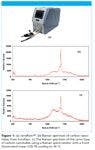
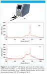
Figure 1
Conclusions
B&W Tek's innoRam Raman spectrometer system, featuring a back-thinned 2D vertically binned CCD detector with TE-cooling to –20 °C, provides research-grade performance with high sensitivity and SNR, which is clearly demonstrated by the comparison of Raman analysis of carbon nanotubes between innoRam and a Raman system using a conventional front-illuminated linear CCD with TE-cooling to 14 °C.


B&W Tek, Inc.
19 Shea Way, Newark, DE 19713
Tel. (302) 368-7824, Fax: (302) 368-7830
Website: www.bwtek.com, Email: info@bwtek.com


Single Cell and Microplastic Analysis by ICP-MS with Automated Micro-Flow Sample Introduction
April 25th 2024Single cell ICP-MS (scICP-MS) is increasingly seen as a powerful and fast tool for the measurement of elements in individual cells, mainly due to the high sensitivity and selectivity of ICP-MS. Analysis is performed in the same way as single nanoparticle (spICP-MS) analysis, which has become a well-established technique for the analysis of nanoparticles and particles.
Hot News on Agilent LDIR, New Developments, and Future Perspective
April 25th 2024Watch this video featuring Darren Robey and Dr. Wesam Alwan from Agilent Technologies to gain insights into the future trends shaping microplastics research and the challenges of their characterization. Discover the essential components necessary for accurate microplastics analysis and learn how the Agilent 8700 LDIR system addresses these challenges. Offering rapid and precise analysis capabilities, along with easy sample preparation methods that minimize contamination, the Agilent 8700 LDIR system is at the forefront of advancing microplastics research.
The World of Microplastics Up to Date – an Overview
April 23rd 2024Watch this 20-minute educational video by Andreas Kerstan, Agilent Product Specialist in molecular spectroscopy, to gain a comprehensive update on the microplastics landscape and the environmental concerns related to them. Discover the current challenges in microplastics characterization and how Agilent innovative solutions and techniques, including FTIR, LDIR, GC/MS, and ICP-MS, are addressing these issues head-on.

