EDAX Inc.
EDAX headquarters is located in Mahwah, New Jersey, housing sales, engineering, technical support, and operations. EDAX is committed to providing the best possible support for our customers world-wide with sales, service, and applications support offices located in Japan, China, Singapore, The Netherlands, Germany, the United Kingdom, and the United States.
Company Description
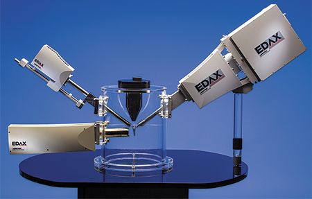
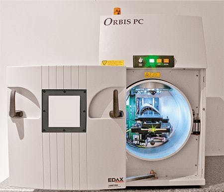
EDAX is a leading provider of innovative materials characterization systems encompassing energy dispersive spectrometry (EDS), wavelength dispersive spectrometry (WDS), electron backscatter diffraction (EBSD), and micro X-ray fluorescence (XRF). EDAX products include standalone tools for EDS, EBSD, and WDS, integrated tools for EDS/EBSD, EDS/WDS, and EDS/EBSD/WDS, and a free-standing micro-XRF bench-top elemental analyzer providing small and micro-spot X-ray analysis and mapping. EDAX develops the best solutions for micro- and nano-characterization, where elemental and/or structural information is required, making analysis easier and more accurate. EDAX designs, manufactures, distributes, and services products for a broad range of industries, educational institutions, and research organizations.


Chief Spectroscopic Techniques Supported
- Energy dispersive spectroscopy (EDS)
- Energy dispersive X-ray fluorescence (Micro-XRF)
- Electron backscatter diffraction (EBSD)
- Wavelength dispersive spectroscopy (WDS)
Markets Served
EDAX instrumentation for elemental and structural analysis is found in a broad spectrum of industrial, academic, and government applications from the field or production line to the most advanced research and development laboratory. Typical markets served include semiconductor and microelectronics, academic and industrial R&D laboratories, RoHS/WEEE, renewable energy, pharmaceuticals, mining, security, forensics, catalysts, petrochemicals, metallurgy, and manufacturing operations.
Major Products/Services
- Energy dispersive X-ray fluorescence: EDAX manufactures micro-XRF analyzers for the laboratory.
- Electron backscatter diffraction: EDAX supplies instrumentation for materials structural analysis on SEM electron-beam microscopes.
- Energy dispersive spectroscopy: EDAX provides a full range of EDS products for elemental analysis on SEM and TEM electron-beam microscopes.
- Wavelength dispersive spectroscopy: EDAX offers parallel beam WDS products for elemental analysis on SEM electron-beam microscopes.
- Fluorescent X-ray detectors: EDAX supplies silicon drift detectors and Si{Li} detectors, which are capable of handling count rates of over 1,000,000 cps and parallel beam wavelength dispersive spectrometers.


Facility
EDAX headquarters is located in Mahwah, New Jersey, housing sales, engineering, technical support, and operations. EDAX is committed to providing the best possible support for our customers world-wide with sales, service, and applications support offices located in Japan, China, Singapore, The Netherlands, Germany, the United Kingdom, and the United States.


EDAX Inc.
91 McKee Drive
Mahwah, NJ 07430
TELEPHONE
(201) 529-4880
FAX
(201) 529-3156
E-MAILinfo.edax@ametek.com
WEB SITEwww.edax.com
YEAR FOUNDED
1962


Getting accurate IR spectra on monolayer of molecules
April 18th 2024Creating uniform and repeatable monolayers is incredibly important for both scientific pursuits as well as the manufacturing of products in semiconductor, biotechnology, and. other industries. However, measuring monolayers and functionalized surfaces directly is. difficult, and many rely on a variety of characterization techniques that when used together can provide some degree of confidence. By combining non-contact atomic force microscopy (AFM) and IR spectroscopy, IR PiFM provides sensitive and accurate analysis of sub-monolayer of molecules without the concern of tip-sample cross contamination. Dr. Sung Park, Molecular Vista, joined Spectroscopy to provide insights on how IR PiFM can acquire IR signature of monolayer films due to its unique implementation.


Deep Level Transient Spectroscopy Reveals Influence of Defects on 2D Semiconductor Devices
April 25th 2024A recent study used deep level transient spectroscopy to investigate the electrical response of defect filling and emission in monolayer metal-organic chemical vapor deposition (MOCVD)-grown materials deposited on complementary metal-oxide-semiconductor (CMOS)-compatible substrates.

