|Articles|March 1, 2016
- Spectroscopy-03-01-2016
- Volume 31
- Issue 3
Selecting an Excitation Wavelength for Raman Spectroscopy
Author(s)David Tuschel
Were it not for the problem of photoluminescence, only one laser excitation wavelength would be necessary to perform Raman spectroscopy. Here, we examine the problem of photoluminescence from the material being analyzed and the substrate on which it is supported. Selecting an excitation wavelength that does not generate photoluminescence reduces the noise level and yields a Raman spectrum with a superior signal-to-noise ratio. Furthermore, we discuss the phenomenon of resonance Raman spectroscopy and the effect that laser excitation wavelength has on the Raman spectrum.
Advertisement
Were it not for the problem of photoluminescence, only one laser excitation wavelength would be necessary to perform Raman spectroscopy. Here, we examine the problem of photoluminescence from the material being analyzed and the substrate on which it is supported. We describe how to select an excitation wavelength that does not generate photoluminescence, reduces the noise level, and yields a Raman spectrum with a superior signal-to-noise ratio. Furthermore, we discuss the phenomenon of resonance Raman spectroscopy and the effect that laser excitation wavelength has on the Raman spectrum.
One of the most frequent questions that I hear from people new to Raman spectroscopy is, “What laser excitation wavelength do I need?” Of course, the answer to that question is that it depends entirely upon the materials one wishes to analyze. The Raman scattering cross-section of the material is important and so too are its physical and optical properties. For example, if the sample is transparent to the excitation wavelength and thin enough, one can expect a spectral contribution from the substrate on which the sample is mounted or positioned. And that spectral contribution can be either Raman scattering or photoluminescence.
Let’s work through some of the considerations relevant to choosing a laser excitation wavelength for Raman spectroscopy. To begin with, one should be aware that the Raman scattering strength is proportional to the fourth power of the excitation frequency, ν4exc. Consequently, one can expect to obtain a much stronger Raman signal from a given sample when using a higher excitation frequency. The frequency of the light is inversely proportional to the wavelength, and so all other things being equal, the shorter excitation wavelength will yield a stronger Raman signal. That is one of the reasons why, when given a choice, Raman spectroscopists prefer shorter excitation wavelengths.
Another consideration when selecting an excitation wavelength can be the variation of the optical density of the material as a function of wavelength. If the material is transparent, then the depth of focus and focal volume of the laser beam will be dictated by the numerical aperture of the lens, the wavelength of the laser light, and the real component of the sample’s refractive index at that wavelength. However, if the sample is not transparent (that is, the imaginary component of the refractive index of the sample is nonzero), then the depth of light penetration will be dictated not by the physical optics but by the absorptivity of the sample at that wavelength. These circumstances have allowed many spectroscopists to perform depth profiling of materials such as semiconductors by changing the excitation wavelength. In general, the longer the excitation wavelength the deeper into the sample the light penetrates. The variation of depth penetration in semiconductors afforded by the range of commercially available visible wavelength lasers conveniently matches the depths to which certain microelectronic devices have been fabricated. The variation of depth penetration in the visible region has allowed Raman spectroscopists to perform depth profiles in ion implanted Si merely by changing the excitation wavelength (1–4).
In some structures, it is essential to control the depth of penetration to constrain the analysis to a thin film at the surface. This is particularly true when analyzing strained Si. A common structure is to have a thin strained Si layer grown on a SiGe layer that is on a strain-free Si substrate. If the excitation wavelength is too long, the laser light will penetrate through the strained Si and SiGe to the strain-free Si substrate. The deeper the penetration of the laser light, the greater the fractional contribution of the substrate Si to the overall Raman signal and spectrum. The result is that the much stronger substrate Si signal overwhelms the much weaker signal from the very thin strained Si. Consequently, the strained Si Raman scattering is buried in the substrate signal at 520.7 cm-1. To resolve the strained Si signal from that of the substrate Si one needs to limit the depth of penetration of the laser light. Therefore, most analyses of thin strained Si structures built on a Si substrate require excitations wavelengths in the violet region or shorter.
Lateral spatial resolution is another consideration when selecting an excitation wavelength. Increasingly, Raman spectroscopy is being done on the micrometer scale using Raman spectrometers coupled to optical microscopes. The need to analyze samples whose chemical composition or solid state structure varies on a micrometer spatial scale is driving the use of micro-Raman spectroscopy. Here, spatial resolution of the measurement is important and one needs a laser spot size commensurate with the spatially varying structure to be analyzed. Consequently, when selecting an excitation wavelength you should know that the size of the focused laser beam is diffraction limited and dependent upon the laser wavelength. The Airy disk diameter (the ideal laser spot size [DAiry]) and spatial resolution (p) for the micro-Raman configuration are given by the following expressions:
where λ is the wavelength of light and NA is the numerical aperture of the microscope objective. Therefore, the choice of excitation wavelength directly affects the spatial resolution of micro-Raman measurements. For example, the diffraction limited spatial resolutions for excitation at 532 nm and 785 nm are 360 nm and 530 nm, respectively. Of course, these values represent the ideal and actual spatial resolution will depend on the quality and alignment of your optics.
The Photoluminescent Background
Anyone having had any experience with Raman spectroscopy will tell you that fluorescence is the nemesis of Raman spectroscopists. Even if the primary substance in the sample does not itself emit, even trace impurities can cause enough photoluminescence to overwhelm the Raman signal. The principal reason for this problem is that emission is a one photon process whereas Raman scattering is a two photon process; that is, photoluminescence has a much higher probability of occurring than does Raman scattering. Related to that fact, you have perhaps heard the oft given explanation of the weak Raman effect and how in general only one Raman photon is generated for every 106 to 109 photons incident upon the sample. Therefore, the presence of a fluorophore with even extremely low quantum efficiency can produce an emission that overwhelms the Raman signal.
You may be asking yourself why a simple background subtraction of the photoluminescent component wouldn’t be sufficient to reveal the remaining Raman spectrum if the Raman and photoluminescent signals are superimposed. The problem is that the background photoluminescence can be so great that the noise generated by this signal is on the order of or even greater than the Raman signal alone. Consequently, software treatment of the data or any other experimental mechanism that does not eliminate the photoluminescent background from the raw signal generally does not produce results as good as those for which no photoluminescent background is present. To avoid the photoluminescence background and the noise that it produces one should identify an excitation wavelength that does not induce photoluminescence in the sample either from the principal component or even trace impurities. That is why old school Raman spectroscopists always want as many laser wavelengths as possible available to them when working with a variety of materials.
Many samples that appear transparent will nevertheless yield a photoluminescent background, sometimes so strong that nothing but photoluminescence is observed in the Raman spectrum. One finds that this is often the case with commercial polymers, even those that are colorless and transparent. The polymers themselves are very often transparent with absorption because of electronic transitions generally occurring in the ultraviolet region of the spectrum. Polymers that are colored often appear that way because of dyes or colorants added to the polymer in the manufacturing process. One might expect the colorless and transparent commercial polymers to yield a photoluminescence free Raman spectrum without any significant background. However, that is very often not the case. You may try to obtain a Raman spectrum using 532-nm excitation of a colorless, transparent plastic bottle that had contained a beverage or other commercial product and you will very likely generate a strong photoluminescence in the region where you expect to detect Raman scattering. Moreover, you may find while observing the spectrum in real time display that the photoluminescent background diminishes over time with continued illumination. This familiar phenomenon is termed photobleaching and has been used extensively in the past decades by Raman spectroscopists to obtain a Raman spectrum with a good signal-to-noise ratio, far better than the one that existed upon initial illumination. The justification for using photobleaching is the premise that the photoluminescence is not from the polymer itself but from additives or minority components that are still present from the polymerization process or were added for other reasons such as stabilization or brightening. If the Raman spectrum of the bulk polymer remains essentially the same over the time of the photobleaching and the measurement, then the assumption that the photobleaching is the result of photolysis of minority components would seem reasonable. There is a bit of craft involved in photobleaching and only laboratory experience will teach you the right conditions (laser power density, duration of laser exposure) for successfully photobleaching a polymer or other sample to remove background photoluminescence without altering or completely degrading the material of interest. One must apply photobleaching with great care to be sure that the Raman spectrum that you acquire is that of the original polymer or bulk material and not that of a laser-induced photolysis product.
Photobleaching may not always be a reasonable or acceptable procedure for acquiring a Raman spectrum. There are times when even continued laser illumination at low power density over even tens of minutes will not remove the photoluminescent background. If that is the case, you need to try a different excitation wavelength. The thinking behind selecting a different excitation wavelength is to use one for which the absorptivity is much lower and thereby yields much less photoluminescence. Think of this as trying to move your Raman laser source out of the absorption spectrum or excitation profile that is the source of the photoluminescence of the sample. The default selection is to a longer excitation wavelength. The assumption is that there will be less absorption if any at all and therefore generate weaker or no photoluminescence.
A sample of commercially available polystyrene pipe demonstrates this concept fairly effectively. Spectra of this sample were acquired using 532-, 638-, and 785-nm excitation and are shown in Figure 1. Clearly, the polystyrene Raman bands can be observed in all of the spectra and the photoluminescence does not preclude one from obtaining a good Raman spectrum using any of these excitation wavelengths. However, you can see that 532-nm excitation yields the greatest photoluminescent background and accompanying noise. Close examination of the spectra reveals greater noise in the Raman component of the 532-nm excited spectrum than is observed when using either 638-nm or 785-nm excitation. The spectral noise demonstrates the essential problem associated with the acquisition of a Raman spectrum over a wavelength region where photoluminescence also occurs. If the emission is too strong, the Raman bands may be lost in the noise and simply not observed in the photoluminescence spectrum.
Figure 1: Raman spectra of commercial polystyrene pipe obtained using excitation wavelengths of 532 nm (red spectrum), 638 nm (blue spectrum), and 785 nm (black spectrum).
We stated earlier that the traditional approach to avoiding photoluminescence once it has been detected with one excitation wavelength is to change to another at a longer wavelength. The reasoning behind that protocol is based on the premise that one may be moving out of an absorption band or excitation manifold of the material. Of course, that does not always work because by changing to a longer excitation wavelength one may “move out” of one excitation manifold only to “move in” to another from perhaps the same or a different chemical compound in the sample. The move to longer excitation wavelength is effective with our sample of polystyrene pipe. You see that using 638-nm excitation has moved our Raman spectrum into the long wavelength tail of the photoluminescence. Consequently, the photoluminescence is much weaker, there is less of a background, and the signal-to-noise of the Raman component of the spectrum is much better. Finally, using 785-nm excitation generates no discernible photoluminescence. Consequently, the Raman spectrum has no background and a very good signal-to-noise ratio.
I stated above that the selection of a longer wavelength was intended to “move out” of an excitation manifold. Actually, one might say that there are two moves occurring when changing to a longer excitation wavelength. There is the move of the laser excitation wavelength out of the photoluminescence excitation manifold and the move of the Raman scattering to the photoluminescence “wavelength tail” or even entirely out of the spectral region of the emission. Figure 2 shows the same spectra from Figure 1 now plotted on an absolute wavelength scale. Here, you can clearly see how the Raman spectrum moves to the photoluminescence wavelength tail when using 638-nm excitation and then completely out of the emission region when using 785-nm excitation. The take-home message here is that by selecting an excitation wavelength that generates little or no photoluminescence the signal-to-noise of the Raman spectrum can be greatly improved. The selection of an excitation wavelength that generates little or no photoluminescence, and thereby reduces the detector noise associated with it, will always produce superior results to methods involving spectral subtraction of the photoluminescent component or other data treatments that still retain the high background detector noise of the original spectral measurements.
Figure 2: Raman spectra of commercial polystyrene pipe obtained using excitation wavelengths of 532 nm (red spectrum), 638 nm (blue spectrum), and 785 nm (black spectrum).
Raman Scattering and Photoluminescence from Glass
The most commonly used substrate when performing micro-Raman spectroscopy is the glass microscope slide. The chemical composition and optical spectroscopic properties of the glass slide are of course not relevant when it functions merely as a support to hold a sample in position that is opaque. However, its spectroscopic properties are important if the sample is transparent to the excitation wavelength. If the transparent sample is thick enough such that the glass slide is completely out of focus, the spectral contribution from the glass slide may be minimal. That is because the laser power density at the glass slide, which is well below the focal plane, will be low. Furthermore, the microscope objective will collect few photons that originate out of focus depending upon the physical optics and light transmission of the sample itself. However, when analyzing thin transparent samples such as polymer films or many biological samples, photoluminescence or Raman scattering from the glass will be detected and the proper choice of alternative substrate can be just as critical as that of the excitation wavelength because of the spectroscopic properties of the glass microscope slide.
In the case of the polystyrene pipe, we saw the advantage of using 785-nm laser excitation to eliminate the photoluminescence generated when using 532-nm light. There are many such samples, particularly in the biosciences, for which 785-nm excitation produces the least amount of photoluminescence. However, we must remember that the laser light will penetrate transparent or translucent samples, particularly if they are thin, and thereby potentially generate Raman scattering and photoluminescence from the underlying substrate. This is where the spectroscopic properties of the glass slide become important. Spectra of a glass microscope slide acquired using 532-, 638-, and 785-nm excitation are shown in Figure 3. The spectrum acquired using 532-nm excitation consists of broad Raman bands from SiO2 with minimal photoluminescence beyond approximately 3200 cm-1. A spectrum from the same glass slide and acquired using 638-nm excitation consists of very strong photoluminescence throughout and peaking at approximately 3000 cm-1. A sense of how strong the photoluminescence is can be ascertained by the weakness of the Raman bands relative to that of the photoluminescence. Finally, a spectrum of the glass slide acquired using 785-nm excitation consists of a very strong and broad photoluminescence peaking at approximately 1400 cm-1 and completely obscuring the fingerprint region of the Raman spectrum. Here again, the Raman bands of glass can barely be detected above the strong photoluminescence generated by the illumination with 785-nm light. In this trend, we encounter the exact opposite wavelength dependent response that we observed for the commercial polystyrene pipe; the photoluminescence from glass varies and grows stronger with increasing excitation wavelength!
Figure 3: Raman spectra of glass microscope slide obtained using excitation wavelengths of 532 nm (red spectrum), 638 nm (blue spectrum), and 785 nm (black spectrum).
Of course, we want to choose the excitation wavelength based upon the best response from the sample and not from the substrate. Clearly, then, we want to find an alternative to the glass microscope slide. If a transparent substrate is needed, commercially available fused quartz substrates meet that need very nicely. Raman spectra of fused quartz obtained using 532-, 638-, and 785-nm excitation are shown in Figure 4. All three spectra appear the same consisting of strong Raman scattering only at Raman shifts less than 500 cm-1 and there is no photoluminescence. Therefore, if a transparent substrate is needed, fused quartz should be chosen instead of the glass microscope slide for micro-Raman analyses of biological samples, thin polymer films, or any other transparent sample whose Raman scattering is weak relative to that of glass. Don’t forget that the glass yields significant Raman scattering out to approximately 1200 cm-1, so the fused quartz may still offer some advantages over a glass microscope slide even when using 532-nm excitation. And certainly fused quartz is the only sensible choice when a transparent substrate is needed and one is using 785-nm excitation.
Figure 4: Raman spectra of fused quartz obtained using excitation wavelengths of 532 nm (red spectrum), 638 nm (blue spectrum), and 785 nm (black spectrum).
Resonance Raman Spectroscopy of Pentacene
Resonance Raman spectroscopy can provide significantly enhanced signals over normal Raman scattering from the same sample. The resonance enhancement is achieved when using an excitation wavelength that is in resonance with an electronic transition of the compound. Those vibrational modes that are coupled to this electronic transition will be resonantly enhanced and their Raman bands will appear much stronger relative to those bands of vibrational modes not coupled to the electronic transition. Consequently, Raman spectra obtained from one compound and even a single sample can appear different depending upon whether the laser excitation is in resonance with an electronic transition of the material. This is a very important point. Raman spectroscopists must be aware of the potential for resonance effects in their spectra particularly when comparing them to those acquired with other excitation wavelengths or Raman spectra of the same material published in the literature.
Pentacene is a dark colored organic compound showing great promise for its use in molecular electronic devices, particularly organic field effect transistors. Attempts to understand the conduction mechanism and the role that chemical bonding and crystal structure play in that process can be assisted by the use of resonance Raman spectroscopy. In particular, Franck-Condon processes can be probed through the resonance Raman effect (5). Absorption in pentacene occurs broadly between 500 and 725 nm with maxima at approximately 550, 575, 625, and 675 nm (6). Consequently, one can couple in to these electronic transitions to generate resonance-enhanced Raman spectra using the appropriate excitation wavelengths.
We have probed individual grains of pentacene obtaining micro-Raman spectra from single locations on a given grain using different excitation wavelengths at each location. The variation in the Raman spectra from a single location acquired using different excitation wavelengths reveals the coupling between the phonons and electronic transitions. Raman spectra acquired using 473-, 532-, 633-, and 785-nm excitation are shown in Figure 5. Some of the band positions are labeled to help the reader note the differences in relative intensities of the Raman bands for the various excitation wavelengths. Note how different the overall spectra appear dependent upon the excitation wavelength. Nevertheless, careful examination of the spectra reveals that the same Raman bands are present in all of the spectra. What varies with excitation wavelength are the relative intensities of the Raman bands. As we said earlier, those vibrational modes coupled to the electronic transition will yield enhanced Raman scattering. Therefore, the correct identification of the vibrational modes and assignment of the Raman bands that undergo enhancement can provide insight into the chemical bonds involved in an electronic transition at a specific wavelength. Much can be said about the chemical bonding and photophysics of pentacene, as revealed in Figure 5. However, that detail is beyond the scope of this publication. The important lesson here is to recognize and understand the importance of excitation wavelength when the potential exists for resonance Raman effects.
Figure 5: Raman spectra acquired from a single location on an individual grain of pentacene using 473-, 532-, 633-, and 785-nm excitation.
Resonance Raman Spectroscopy of 2D Crystals
Two-dimensional (2D) crystals constitute another class of materials for which the selection of excitation wavelength is important. Two-dimensional crystals are not just small portions of the bulk materials carrying the same properties as those of the three dimensional kind. Rather, their physical, electronic, and spectral characteristics can be significantly different. Specifically, MoS2 in its bulk form is an indirect bandgap semiconductor, whereas in its monolayer to few-layer forms it becomes a direct bandgap semiconductor (7). Splendiani and coworkers (8) have studied exfoliated MoS2 monolayer and few-layer flakes by photoluminescence and have observed direct excitonic transitions. Exciting with 532-nm laser light, they observed broad photoluminescence centered at 627 and 677 nm, whereas these emissions are completely absent when illuminating bulk MoS2. The room temperature bandgap of bulk MoS2 is approximately 1.7 eV (corresponding to 730 nm) with complex excitonic features between 1.7 and 2.5 eV (9).
The crystalline structure of 2H-MoS2 belongs to the D6h crystal class, and factor group analysis predicts one A1g, one E1g, and two E2g Raman active modes (9–15). The symmetry assignments and corresponding Raman band positions for bulk hexagonal MoS2 are: E1g (286 cm-1), E12g (383 cm-1), A1g (408 cm-1), and E22g (32 cm-1). Furthermore, it is important to remember that some visible wavelengths of the laser light used to excite Raman scattering correspond to energies of MoS2 electronic transitions. The absorption spectrum of MoS2 reflects the band gap of 1.7 eV, but it also manifests fine structure with narrow absorption peaks at 1.9 eV (653 nm) and 2.1 eV (590 nm) related to d-to-d orbital transitions split by spin-orbit coupling and designated A1 and B1 excitons, respectively (9,16). Consequently, one can observe an excitation wavelength dependence of the first-order Raman band intensities as well as the appearance of Raman bands assigned to harmonic and combination modes when the laser excitation is of a wavelength that couples into these excitonic transitions (9,13,15,16).
Just as the monolayer to few-layer 2D crystal structure of MoS2 affects the electronic structure, particularly the nature of the bandgap, the vibrational modes are also affected. The first-order Raman bands listed above are for bulk MoS2. However, these bands shift to different energies progressively as the structure changes from approximately six layers down to a single monolayer. The E22g band has been observed to shift progressively from 32 cm-1 in the bulk to 23 cm-1 in the single trilayer (17). The term trilayer derives from the fact that MoS2 is not a planar compound, that is, the Mo and S atoms are not all in the same plane. So, a plane of S atoms can be envisioned on the surface with a plane of Mo atoms above that plane and another plane of S atoms above the Mo one, hence the term trilayer. Also, the band positions and respective separations of the E12g and A1g bands show progressive changes from the bulk to a single layer. The E12g (383 cm-1) band shifts to higher wavenumbers and the A1g (408 cm-1) band shifts to lower wavenumbers in progressing from the bulk to a single trilayer corresponding to a band separation of 25 cm-1 to 19 cm-1, respectively (18).
The changes of Raman band position with the number of molecular layers described above are most readily observed when using 532-nm or shorter wavelength excitation. The Raman spectra obtained when using 632.8-nm light to excite few-layer MoS2 appear quite different because of coupling with the aforementioned A1 excitonic transition and the subsequent resonance enhancement. The activity of the harmonic and combination modes yields a richer spectrum and the determination of the number of trilayers present is determined from both changes in band shape and relative intensities (19,20).
Exfoliated few-layer flakes of MoS2 are typically heterogeneous, and so the Raman and photoluminescence spectra tend to spatially vary on the flake. Nevertheless, there are spectra that can be considered representative of few-layer MoS2 and they are shown in Figure 6. These spectra were acquired at the same location from the interior of a MoS2 flake, but with different excitation wavelengths. That spectrum acquired with 532-nm excitation is typical of those reported in the literature; it consists primarily of the E12g band at 383 cm-1 and the A1g band at 408 cm-1 as well as the Si substrate Raman band at 520 cm-1. In contrast, the spectrum generated with 632.8-nm excitation is striking insofar as it consists of the same first order bands and those due to harmonics and combination modes. Remember that the absorption spectrum of MoS2 contains fine structure with narrow absorption peaks at 1.9 eV (653 nm) and 2.1 eV (590 nm) related to d-to-d orbital transitions split by spin-orbit coupling and designated A1 and B1 excitons, respectively (9,16). Consequently, the 632.8-nm excitation couples into the A1 transition producing a resonance enhancement of all of the additional modes observed in Figure 6. All of the bands in the spectrum excited with 632.8-nm light can be accounted for and have previously been assigned (9,13,16).
Figure 6: Raman spectra of few-layer MoS2 flake taken at the same location with different excitation wavelengths. The band at 520 cm-1 corresponds to the substrate Si.
Conclusions
The selection of excitation wavelength for Raman spectroscopy has been examined within the context of photoluminescence that obscures the Raman bands and resonance enhancement of Raman signal strength. Photoluminescence from either the sample or the substrate produces detector noise on the order of or even greater than the Raman signal itself. The problem is that the background photoluminescence can be so great that the noise generated by this signal is on the order of or even greater than the Raman signal alone, thus obscuring the Raman component. The selection of an excitation wavelength that generates little or no photoluminescence, and thereby reduces the detector noise associated with it, will always produce superior results. Resonance Raman spectroscopy can provide significantly enhanced signals over normal Raman scattering from the same sample. Raman scattering from those vibrational modes coupled to the electronic transition is enhanced when using the appropriate excitation wavelength. Consequently, Raman spectra obtained from one compound and even a single sample can appear different depending upon whether the laser excitation is in resonance with an electronic transition of the material.
References
- P.X. Zhang, I.V. Mitchell, P.J. Schultz, and D.J. Lockwood, J. Raman Spec.25, 515–520 (1994).
- A.C. deWilton, M. Simard-Normandin, and P.T.T. Wong, J. Electrochem. Soc.133, 988–993 (1986).
- J.P. Lavine and D.D. Tuschel, Mat. Res. Soc. Symp. Proc.588, 149–154 (2000).
- D.D. Tuschel and J.P. Lavine, Mat. Res. Soc. Symp. Proc.438, 143–148 (1997).
- R. He, N.G. Tassi, G.B. Blanchet, and A. Pinczuk, Phys. Rev. B83, 115452 (2011).
- A. Rao, M.W.B. Wilson, S. Albert-Seifried, R. Di Pietro, and R.H. Friend, Phys. Rev. B84, 195411 (2011).
- K.F. Mak, C. Lee, J. Hone, J. Shan, and T.F. Heinz, Phys. Rev. Lett.105, 136805 (2010).
- A. Splendiani, L. Sun, Y. Zhang, T. Li, J. Kim, C.-Y. Chim, G. Galli, and F. Wang, Nano Lett.10, 1271–1275 (2010).
- A.M. Stacy and D.T. Hodul, J. Phys. Chem. Solids46, 405–409 (1985).
- J.R. Ferraro, Appl. Spec.29, 418–421 (1975).
- S. Jimenez Sandoval, D. Yang, R.F. Frindt, and J.C. Irwin, Phys. Rev. B44, 3955–3962 (1991).
- T.J. Wieting and J.L. Verble, Phys. Rev. B3, 4286–4292 (1971).
- J.M. Chen and C.S. Wang, Solid State Commun. 14, 857–860 (1974).
- S. Sugai and T. Ueda, Phys. Rev. B26, 6554–6558 (1982).
- D.O. Dumcenco, K.Y. Chen, Y.P. Wang, Y.S. Huang, and K.K. Tiong, J. Alloys Compounds506, 940–943 (2010).
- B.C. Windom, W.G. Sawyer, and D.W. Hahn, Tribol. Lett.42, 301–310 (2011).
- Y. Zhao, X. Luo, H. Li, J. Zhang, P.T. Araujo, C.K. Gan, J. Wu, H. Zhang, S.Y. Quek, M.S. Dresselhaus, and Q. Xiong, Nano Lett.13, 1007–1015 (2013).
- C. Lee, H. Yan L.E. Brus, T.F. Heinz, J. Hone, and S. Ryu, ACS Nano4, 2695–2700 (2010).
- K. Golasa, M. Grzeszczyk, R. Bozek, P. Leszczynski, A. Wysmolek, M. Potemski, and A. Babinski, Solid State Commun. 197, 53–56 (2014).
- B. Chakrabory, H.S.S. Ramakrishna Matte, A.K. Sood, and C.N.R. Rao, J. Raman Spectrosc.44, 92–96 (2013).
David Tuschel is a Raman applications manager at Horiba Scientific, in Edison, New Jersey, where he works with Fran Adar. David is sharing authorship of this column with Fran. He can be reached at:
Articles in this issue
over 10 years ago
2016 Salary Survey: Continuing the Squeezeover 10 years ago
A Convenient Alternative to MALDI and ESIover 10 years ago
Vol 31 No 3 Spectroscopy March 2016 Regular Issue PDFAdvertisement
Related Content
Advertisement


Advertisement
Advertisement
Trending on Spectroscopy Online
1
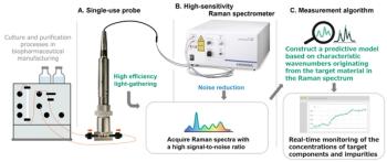
Fujifilm, Horiba Unveil New Inline Raman System
2
Where is Raman Spectroscopy Delivering the Most Value for Real-Time Chemical Analysis in Oil and Gas?
3
Best of the Week: Prebiotic Chemistry, Real-Time Chemical Analysis, Previewing ISMS 2026
4
Exploring Emerging Photophysical Phenomena
5