Topographic Confocal Raman Imaging using True Surface Microscopy
Application Notebook
True surface microscopy for topographic confocal Raman imaging adds optical profilometer functionality to a highly sensitive confocal Raman microscope. Using this profilometer function, topographic scans of several square millimeters can be acquired, similar to a very large AFM topography image. This acquired large-area topography image can be used to trace the surface contours while acquiring a confocal Raman image.
True surface microscopy for topographic confocal Raman imaging adds optical profilometer functionality to a highly sensitive confocal Raman microscope. Using this profilometer function, topographic scans of several square millimeters can be acquired, similar to a very large AFM topography image. This acquired large-area topography image can be used to trace the surface contours while acquiring a confocal Raman image.
A wide variety of Raman Imaging applications greatly benefit from a confocal setup (1), and depth scans as well as 3D images are only possible due to high confocality (2) especially when combined with diffraction-limited lateral resolution. On rough or inclined samples, however, such a high level of confocality can cause part of the scanned area to be out of focus. This is especially true for larger scans on the mm scale because it can become quite a challenge to achieve a flatness of only a few µm over such a large area. Decreasing the confocality and thus making the system less sensitive to variations due to a lower depth resolution is a solution if the topographic changes are small (for example <10 µm), but even in those cases it is not desirable due to the loss in surface sensitivity.


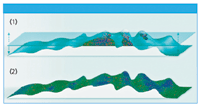
Figure 1: (1): Confocal Raman imaging on large samples (mm-size) delivers an optical cross-section through the sample. If the sample is not transparent, only the intersection of focal plane and sample surface will give a Raman signal. Depending on the objective used, the focal plane might have a thickness of less than 1 µm. (2) The true surface microscopy option enables the precise tracing of the surface while acquiring Raman imaging data, resulting in a true surface Raman image.
Especially when looking at intensity changes of peaks or when working with transparent samples, this option should be avoided. However, without such a compromise or if the topographic variation is too large, it is only possible to image a slice of the sample in one scan in conventional Confocal Raman Imaging systems (Figure 1.1). For samples with high optical density for the wavelength of choice (= low penetration depth) one could in this fashion acquire many slices and then reconstruct the surface, but this would be a very time consuming procedure. Confocal Raman Imaging in combination with true surface microscopy on the contrary allows the user to remain in focus on the surface at every point and thus acquire the complete image in one scan (Figure 1.2). True Surface microscopy uses the principle of a confocal chromatic sensor as shown in Figure 2. Scanning the sample in the XY plane reveals a topographic map of the sample. Such a map can be followed in a subsequent confocal Raman image scan so that the Raman excitation is always kept in focus with the sample surface (or at any chosen distance below the surface).

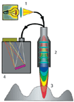

Figure 2: The functionality of a confocal chromatic sensor. White light (1) is focused through a hyperchromatic lens system (2) onto the sample (3) and only the light scattered in its focal plane reaches the spectrometer (4) with high intensity (yellow in the example shown here).
Results
In order to illustrate the advantage of such a sensor a highly inclined and very rough geological sample was investigated with true surface microscopy. A photograph of the sample (Josefsdal Chert 99SA07, courtesy of Frances Westall, CNRS Orleans, France) can be seen in Figure 3.1 and the result of the topographic measurement in Figure 3.2. The scanned area was 2 × 2 mm with a maximum topographic range in the scanned area of approximately 1.3 mm. If such an area is scanned in confocal Raman imaging mode without correction of the topography only a very limited range can be recorded, which is illustrated in Figure 3.3. The same area was also scanned with the topographic data taken into account in order to adjust the Z-position at each image pixel such that the surface is in focus. The results (Figure 3.4) clearly show much more detailed information of the sample surface. The colors in Figure 3.3 and 3.4 match the colors of the corresponding spectra shown in Figure 3.5. Quartz (blue), kerogen (green) as well as anatase (red) could be found in this sample. Areas marked in yellow indicate high levels of fluorescence. The confocal Raman images were generated using single- as well as multivariate data analysis methods as example described in (1).


Figure 3
Conclusion
Combining true surface microscopy with confocal Raman microscopy allows for the first time the investigation of irregularly shaped surfaces with high confocality. Sample preparation which may require a substantial amount of time and experimental know-how in order to avoid unwanted artifacts, is reduced to a minimum. Samples that previously could not be recorded because they could not be prepared in the required way due to sample destruction are now also accessible for large area confocal Raman microscopy.

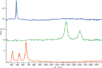
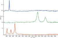
Figure 4: Corresponding spectra of the mineral phases: blue: quartz, green: kerogen, red: anatase.
References
(1) T. Dieing, O. Hollricher, and J. Toporski, Eds., Confocal Raman Imagingm (Springer, Berlin/Heidelberg, 2010).
(2) http://www.witec.de/en/download/Raman/WITec_3DRamanImaging.pdf.
WITec Instruments Corp.
122 McCammon Ave., Maryville, TN 37804
tel. (865) 984-4445, fax (865) 984-4441
Email: info@witec-instruments.com
Website: www.WITec-Instruments.com


Single Cell and Microplastic Analysis by ICP-MS with Automated Micro-Flow Sample Introduction
April 25th 2024Single cell ICP-MS (scICP-MS) is increasingly seen as a powerful and fast tool for the measurement of elements in individual cells, mainly due to the high sensitivity and selectivity of ICP-MS. Analysis is performed in the same way as single nanoparticle (spICP-MS) analysis, which has become a well-established technique for the analysis of nanoparticles and particles.
Hot News on Agilent LDIR, New Developments, and Future Perspective
April 25th 2024Watch this video featuring Darren Robey and Dr. Wesam Alwan from Agilent Technologies to gain insights into the future trends shaping microplastics research and the challenges of their characterization. Discover the essential components necessary for accurate microplastics analysis and learn how the Agilent 8700 LDIR system addresses these challenges. Offering rapid and precise analysis capabilities, along with easy sample preparation methods that minimize contamination, the Agilent 8700 LDIR system is at the forefront of advancing microplastics research.
The World of Microplastics Up to Date – an Overview
April 23rd 2024Watch this 20-minute educational video by Andreas Kerstan, Agilent Product Specialist in molecular spectroscopy, to gain a comprehensive update on the microplastics landscape and the environmental concerns related to them. Discover the current challenges in microplastics characterization and how Agilent innovative solutions and techniques, including FTIR, LDIR, GC/MS, and ICP-MS, are addressing these issues head-on.

