|Articles|April 1, 2018
- Spectroscopy-04-01-2018
- Volume 33
- Issue 4
X-ray Photoelectron Spectroscopy Analysis of the Enhanced Corrosion Resistance of Thermally Oxidized Stainless Steel
Author(s)Nak-Kwan Chung
Although recent steel coating methods have demonstrated improvements in corrosion resistance, they can prove expensive and complicated. In this study, XPS analysis was used to evaluate the corrosion resistance of steel treated with an alternative technique.
Advertisement
The corrosion resistance characteristics of thermally oxidized stainless steel 316 in an ultrahigh vacuum were examined by exposing this material to an inductively coupled plasma. The CF4–O2–Ar mixed plasma used was generated at 1 mTorr with a constant gas mixing ratio of 9:6:5 sccm. Observations by atomic force microscopy (AFM) demonstrated that after plasma etching oxidized the stainless steel, it retained a smooth surface, while moss-like features formed on the surface of stainless steel that was not thermally oxidized. X-ray photoelectron spectroscopy (XPS) studies revealed that significant amounts of Cr2O3 remained on the oxidized surfaces after plasma etching, whereas Cr2O3 appears to be mostly removed from the unoxidized surfaces after plasma etching. In addition, after plasma etching, the concentration of F on the unoxidized sample was greater than that of the oxidized sample in the near surface region according to XPS depth profiling data. Finally, it was found that the 2-nm-thick Cr2O3 passivation film formed on the oxidized stainless steel surface acted as a barrier to penetration of the fluorine during plasma etching, indicating that the oxidized stainless steel is more corrosion resistant than the unoxidized stainless steel.
The process of plasma etching is indispensable for the manufacturing of semiconductor devices in the nanoelectronic era (1–5). During the etching process, a mixture of CF4 and O2 is commonly used as the reactive gas, and the resultant F ions react with Si3N4 and SiO2 layers on the surface of the Si wafer, resulting in the creation of a micropattern (6,7). The reactive gas can also react with the process chamber and vacuum components, which are often composed of stainless steel, resulting in corrosion and deposition of metal contamination on the substrate (8–10). Moreover, reactions with radical ions can occur in the pumping system, and the corrosion of the pumping system causes fluctuations of process parameters such as the pumping speed, leading to lower yields and less reproducibility (11,12). Therefore, to obtain high-quality devices, high corrosion resistance levels of the vacuum components during plasma etching with various gases, radicals, and ions are required.
To improve the corrosion resistance of metals to gases, many researchers have studied various surface treatment technologies by which to passivate metal surfaces (13–19). These approaches involve coating of metal surfaces via physical vapor deposition, chemical vapor deposition, and plasma spraying, among others. In recent work, Wan and colleagues studied Al2O3-layered CrN coatings on the stainless steel substrate by atomic layer deposition (14). They found that the CrN coating acts as a good blocking layer for diffusion of corrosive substances. However, although these coating methods have demonstrated improvements in corrosion resistance, they require expensive and complicated equipment setups.
In our previous studies, uniform and smooth Cr2O3 passivation films were grown on stainless steel surfaces by a simple thermal oxidation method under an ultrahigh vacuum (20–22). The oxide films exhibited remarkable resistance to sorption processes and also served as a diffusion barrier for hydrogen because of their smooth surface and dense structure.
In the present study, we demonstrate the enhanced corrosion resistance of thermally oxidized stainless steel. Cr2O3 films were grown on stainless steel surfaces at 500 °C under oxygen partial pressures of 1 × 10⁻⁸ Torr, after which the surface morphology and chemical composition was investigated after etching with a CF4–O2–Ar plasma. According to atomic force microscopy (AFM) observations, after plasma etching the surfaces of the oxidized stainless steel were much smoother than unoxidized surfaces. X-ray photoelectron spectroscopy (XPS) studies revealed that a large amount of the Cr2O3 film remained on thermally oxidized surfaces after plasma etching, whereas little Cr2O3 remained on the surface of unoxidized samples. In addition, according to XPS depth profiling outcomes, the Cr2O3 films on the passivated stainless steel prevented the formation of metal fluorides and the penetration of F, which is an indicator of corrosion resistance.
Experimental
The substrate samples used in this study were commercial-grade 316 stainless steel with compositions of 18.0 wt% Cr, 10.0 wt% Ni, 2.5 wt% Mo, 2.0 wt% Mn and 0.06 wt% C, and balanced Fe. The 0.5-mm-thick stainless steel sheets used here were cut into 1 cm × 1 cm squares and were ultrasonically cleaned in acetone, followed by ethanol. Subsequently, Cr2O3 passivation films were grown on the stainless steel surfaces in an ultrahigh vacuum chamber with a base pressure of 2 × 10-11 Torr by annealing at 500 °C under an oxygen partial pressure of 1 × 10⁻⁸ Torr. For the corrosion test, the oxidized and the unoxidized stainless steel samples were transferred to a planar inductively coupled plasma (ICP) reactor, as shown schematically in Figure 1. The reactor consisted of a cylindrical chamber with a diameter of 30 cm, a gas controlling system, and a top coil coupled to a 13.56-MHz power supply via a matching network. The samples were etched with CF4–O2–Ar for 10 min with a mixing ratio of 9:6:5 sccm and process pressure of 1 mTorr.
Figure 1: Schematic diagram of the inductively coupled plasma reactor.
The surface morphologies of the etched samples were investigated by AFM (Park System XE 100). The chemical states on the sample surfaces and their compositional depth profiles were also analyzed using XPS (Thermo VG Scientific Sigma Probe) combined with Ar+ ion sputtering. The source type for the XPS analysis was Al Kα with a spot size of 400 µm. Binding energies (BEs) were referenced to the C 1s peak from the carbon surface deposit at 284.6 eV.
Results and Discussion
To analyze the microscopic structure of the samples, AFM measurements were taken, as shown in Figure 2. Before plasma etching, as shown in Figures 2a and 2b, both the oxidized and the unoxidized samples exhibited smooth surfaces with average roughness (Ra) of 1.0 and 2.1 nm, respectively, although some small particles from tens to hundreds of nanometers in size on the unoxidized surface were observed. Figure 2c shows that after etching, the oxidized sample surface remained smooth with an Ra of 1.7 nm. In contrast, it can be observed in Figure 2d that plasma etching produced a mossy and roughened surface with an Ra of 4.5 nm for the unoxidized sample, indicating surface erosion.
Figure 2: AFM images (10 µm × 10 µm) of the stainless steel 316 surfaces before and after plasma etching: (a) the oxidized and (b) the unoxidized stainless steel surfaces before plasma etching, and (c) the oxidized and (d) the unoxidized stainless steel surfaces after plasma etching.
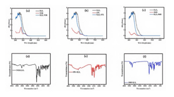
The chemical composition of the sample surfaces before and after plasma etching was evaluated by XPS analysis. Figure 3 shows the changes in the high resolution spectra of the Cr 2p, Fe 2p, and F 1s photoelectron peaks of the thermally oxidized and unoxidized stainless steel samples before and after plasma etching. In Figures 3a and 3b, the Cr 2p3/2 and Cr 2p1/2 spectra can be deconvoluted into three component peaks: those with the highest BEs (CrF2) of 578.2 and 587.6 eV, those at mid-level BEs (Cr2O3) of 576.7 and 586.0 eV, and those with the lowest BEs (metallic Cr) of 574.0 and 583.0 eV (23–25). As shown in Figure 3a, the Cr 2p spectra for the oxidized samples treated with plasma suggest a large decrease of Cr2O3, and a small increase of metallic Cr and CrF2 on the surface. In Figure 3b, the peaks from Cr2O3 on the unoxdized samples after plasma etching are almost not detected. In Figures 3c and 3d, the Fe 2p spectra were deconvoluted into two component peaks: one represents iron oxides such as Fe2O3 and Fe3O4, whose BEs are 710.9 and 724.0 eV, and the other denotes Fe–F chemical bonds whose corresponding BEs are 713.9 and 728.0 eV (26–31). A weak Fe 2p3/2 satellite feature is also observed at 718.8 eV, while no Fe 2p1/2 satellite feature is observed (27,28). It is clear that before plasma etching, a small amount of iron oxide exists on the surface of the oxidized sample, while a significant amount of iron oxide exists on the unoxidized sample surface. After plasma etching, large increases in iron oxides and fluorides were found on the surface of the unoxidized sample relative to that of the oxidized sample. These results are consistent with previous results from Hara and colleagues that the iron oxides underwent involatile fluorination when exposed to the effluent of the plasma, while the surfaces of the Cr2O3 films exposed to the plasma were transformed into volatile fluorides or oxyfluorides, which were then pumped away (8). In Figures 3e and 3f, the F 1s spectra exhibit only one peak at 684.8 eV. That peak can be attributed to metallic fluorides such as FeF3 and CrF2, which formed because of the incorporation of F during plasma etching (24,29,31). After plasma etching, the amount of F on the oxidized stainless steel surface was less than that on the unoxidized stainless steel surface, indicating that the oxidized surface is less eroded than the unoxidized surface.
Figure 3: Comparative XPS spectra of (a-b) Cr 2p, (c-d) Fe 2p, and (e-f) F 1s for the oxidized and unoxidized stainless steel samples before (lower spectrum, black line) and after (upper spectrum, red line) plasma etching, respectively.
The composition as a function of the depth can also be analyzed by XPS with Ar+ ion beam sputtering. Figure 4 shows the results of the XPS depth profiling for the samples before and after plasma etching. In a comparison of Figures 4a and 4b, after thermal oxidation, the concentration of Cr increases from 18.2 at% to 28.5 at% in the surface region, while that of Fe drastically decreases from 10.3 at% to 2.2 at%, resulting in a 2-nm-thick Cr-rich surface film on the oxidized sample. As shown in Figures 4c and 4d, plasma etching reduces the amount of Cr on the surface by 8.5 at% for the oxidized stainless steel and by 16.0 at% for the unoxidized stainless steel, and increases the amount of Fe by 13.0 and 19.5 at% for each sample.
Based on our analysis, we can assess that the change of chemical composition on the topmost surface is closely related to the resistance of corrosion. For the unoxidized stainless steel that is vulnerable to corrosion, the amount of Cr is dramatically decreased after plasma etching. Here it is necessary to compare the compositional change of F and O, which are related to product corrosion after plasma etching. The concentration of F for the unoxidized sample is 35.0 at%, which is about three times larger than that for the oxidized case. In contrast, the concentration of O for the unoxidized sample is 20.0 at%, which is about half as low as that for the oxidized sample. These results show that the initial amount of Cr, which mostly exist in the Cr2O3 before plasma etching, can have a dominant impact on the resistance of corrosion. After plasma etching, the oxidized stainless steel that has enough Cr2O3 film on the surface can effectively prevent the occurrence of fluoride, demonstrating a lower concentration of F than that of F for the unoxidized stainless steel. We can understand this result because a 2-nm-thick Cr2O3 film on a stainless steel surface can effectively prevent the incorporation of F during plasma etching (32).
Figure 4: The XPS depth profiles of (a) the oxidized stainless steel before plasma etching, (b) the unoxidized sample before plasma etching, (c) the oxidized sample after plasma etching, and (d) the unoxidized sample after plasma etching.
Conclusion
In conclusion, the plasma etching resistance levels of thermally oxidized stainless steel surfaces were analyzed by AFM and XPS with Ar+ cluster ion sputtering. According to AFM observations, the surfaces of the oxidized stainless steel remained smooth after plasma etching, while the unoxidized stainless steel surface became rough and had a mossy appearance, indicating surface erosion. It was found that thermal oxidation of stainless steel increased the amount of Cr on the surface, and decreased the amount of Fe, resulting in the formation of a 2-nm-thick Cr2O3 film on the oxidized stainless steel surface. In contrast, plasma etching reduced the amount of Cr on the surface and increased that of Fe. As a result, Cr2O3 on the unoxidized sample surfaces is mostly depleted after plasma etching, while a substantial amount of the Cr2O3 films remains on the thermally oxidized surfaces. In addition, on the topmost surface, the amount of F in the unoxidized stainless steel was found to be much larger than that in the oxidized stainless steel after plasma etching. These findings demonstrate that stainless steel with a Cr2O3 passivation film formed by thermal oxidation provides an improvement in resistance to corrosion for conditions similar to that used in the manufacture of semiconductor devices.
Acknowledgment
The authors gratefully acknowledge the financial support of the Development Program of Measurement Technology for Advanced Ultrathin Film Processing of the Korea Research Institute of Standards and Science and the R&D Convergence Program of National Research Council of Science and Technology (NST, No. CAP-16-04-KRISS).
References
(1) R.J. Shul and S.J. Pearton, Handbook of Advanced Plasma Processing Techniques (Springer-Verlag, Berlin, 2000), pp. 257–259.
(2) D.J. Economou, J. Phys. D 47, 303001 (2014).
(3) M.D. Henry, S. Walavalkar, A. Homyk, and A. Sherer, Nanotechnology 20, 255305 (2009).
(4) G. Oehrlein, R. Phaneuf, and D. Graves, J. Vac. Sci. Technol. B 29, 010801 (2011).
(5) H. Kim, J. Woo, Y. Joo, and C. Kim, Trans. Elecrt. Electron. Mater. 14, 12–15 (2013).
(6) J. Kim, S. Cho, S. Lee, C. Kim, K. Min, and G. Yeom, J. Vac. Sci. Technol. A 31, 061302 (2013).
(7) M. Schaepkens, T. Standaert, N. Rueger, P. Sebel, G. Oehrlein, and J. Cook, J. Vac. Sci. Technol. A 17, 26–37 (1999).
(8) N. Hara, S. Mukuhara, K. Ohtomo, Y. Shimizu, and K. Sugimoto, J. Electrochem. Soc. 149, B297–B305 (2002).
(9) E. Gogolides, V. Constantoudis, G. Kokkoris, D. Kontziampasis, K. Tsougeni, G. Boulousis, M. Vlachopoulou, and A. Tserepi, J. Phys. D 44, 174021 (2011).
(10) H. Jang, A. Efremov, S. Yun, G. Yeom, K. Kim, and K. Kwon, Appl. Surf. Sci. 279, 41–45 (2013).
(11) M. Kitano, H. Ishii, Y. Shirai, and T. Ohmi, J. Vac. Sci. Technol. A 29, 021002 (2011).
(12) J. Okado, K. Okada, A. Ishiyama, Y. Setsuhara, and K. Takenaka, Surf. Coat. Technol. 202, 5595–5598 (2008).
(13) H. Feng, C. Hsu, J. Lu, and Y. Shy, Mater. Sci. Eng. A 347, 123–129 (2003).
(14) Z. Wan, T. Zhang, H. Lee, J. Yang, W. Choi, B. Han, K. Kim, and S. Kwon, ACS Appl. Mater. Interfaces 7, 26716–26725 (2015).
(15) B. Szubzda, A. Antonczak, P. Koziol, L. Lazarek, B. Stepak, K. Lecka, A. Szmaja, and M. Ozimek, IOP Conf. Ser. Mater. Sci. Eng. 113, 012017 (2016).
(16) J. Jones, M. Chen, and Q. Yu, J. Biomed. Mater. Res. B 102, 1363–1374 (2014).
(17) W. Choi, K. Oh, P. Singh, V. Breedveld, and D. Hess, J. Electrochem. Soc. 164, C61–C65 (2017).
(18) S. Maeng, L. Axe, T. Tyson, L. Gladczuk, and M. Sosnowski, Corros. Sci . 48, 21542171 (2006).
(19) F. Martin, M. Lopez, P. Carrera, J. Ramos-Barrado, and D. Leinen, Surf. Interface Anal. 36, 8–16 (2004).
(20) B. Cho, S. Lee, and S. Chung, J. Vac. Sci. Technol. A 14, 2228–2231 (1995).
(21) K. Kim, T. Kang, C. Park, B. Cho, S. Chung, and B. Kim, J. Electron Spectrosc. Relat. Phenom. 101–103, 327–333 (1999)
(22) O.N. Chung, and S. Chung, J. Vac. Sci. Technol. B 21, 1297–1300 (2003).
(23) K. Hanamoto, M. Sasaki, T. Miyashita, Y. Kido, Y. Nakayama, Y. Kawamoto, M. Fujiwara, and R. Kaigawa, Nucl. Instrum. Methods Phys. Res. B 129, 228–232 (1997).
(24) Nurhaerani, K. Arita, Y. Shinonaga, and M. Nishino, Dent. Mater. J. 25, 684–692 (2006).
(25) T. Ohtsuka, M. Ueda, and M. Abe, J. Electrochem. Soc. 163, C459–C469 (2016).
(26) D. Hawn and B. DeKoven, Surf. Interface Anal. 10, 63–74 (1987).
(27) T. Yamashita and P. Hayes, Appl. Surf. Sci. 254, 2441–2449 (2008).
(28) M. Biesinger, B. Payne, A. Grosvenor, L. Lau, A. Gerson, and R. Smart, Appl. Surf. Sci. 257, 2717–2730 (2011).
(29) G. Carraro, A. Gasparotto, C. Maccato, E. Bontempi, O. Lebedev, S. Turner, C. Sada, L. Depero, G. Tendeloo, and D. Barreca, RSC Adv. 3, 23762–23768 (2013).
(30) T. Fujii, F. Groot, G. Sawatzky, F. Voogt, T. Hibma, and K. Okada, Phys. Rev. B 59, 3195–3202 (1999).
(31) H. Ming, J. Ming, S. Oh, S. Tian, Q. Zhou, H. Huang, Y. Sun, and J. Zheng, ACS Appl. Mater. Interfaces 6, 15499–15509 (2014).
(32) M. Aliofkhazraei, Developments in Corrosion Protection (Intech, Croatia, 2014), pp. 41–48.
Nak-Kwan Chung is with the Materials and Energy Measurement Center, at the Korea Research Institute of Standards and Science, in Daejeon, South Korea. Direct correspondence to:
Articles in this issue
over 7 years ago
Ultrafast Lasers in Spectroscopy—Moving into the Mainstreamover 7 years ago
What! I Have to Specify My Spectrometer?over 7 years ago
Market Profile: Process Moisture Instrumentsover 7 years ago
Vol 33 No 4 Spectroscopy April 2018 Regular Issue PDFNewsletter
Get essential updates on the latest spectroscopy technologies, regulatory standards, and best practices—subscribe today to Spectroscopy.
Advertisement
Related Content
Advertisement
![Figure 3: Plots of lg[(F0-F)/F] vs. lg[Q] of ZNF191(243-368) by DNA.](https://cdn.sanity.io/images/0vv8moc6/spectroscopy/a1aa032a5c8b165ac1a84e997ece7c4311d5322d-620x432.png?w=350&fit=crop&auto=format)
Advertisement
Advertisement
Trending on Spectroscopy Online
1
2025 As A Turning Point for Vibrational Spectroscopy: AI, Miniaturization, and Greater Real-World Impact
2
State of the Industry: Spectroscopy at a Crossroads
3
FT-IR Spectroscopy Links Tourism Intensity to Microplastic Pollution in Island Waters
4
A-TEEM–A Fantastic Spectroscopy that Rivals Raman
5