Supplementary Information: Polarized Raman Spectroscopy of Aligned Semiconducting Single-Walled Carbon Nanotubes
Special Issues
This information is a supplementary to the article “Polarized Raman Spectroscopy of Aligned Semiconducting Single-Walled Carbon Nanotubes” that was published in the June 2016 Spectroscopy supplemental issue Raman Technology for Today’s Spectroscopists (1).
This information is supplementary to the article “Polarized Raman Spectroscopy of Aligned Semiconducting Single-Walled Carbon Nanotubes” that was published in the June 2016 Spectroscopy supplemental issue Raman Technology for Today’s Spectroscopists (1).
Optical Anisotropy Calculation in Figure 4
One way of using the Raman imaging data is to obtain an average reading for a larger area of the sample compared to a single point measurement. The boxed areas in Figure 4 represent areas where the Raman spectral measurements were averaged to produce a single Raman spectrum. The boxed area in Figure 4 on the left is an area of unaligned SWCNTs; the boxed area on the right is an area of aligned SWCNTs.
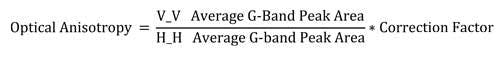
Each boxed area in Figure 4 is 11 x 47 µm (517 sq. µm) with spectra collected at a spatial resolution (pixel size) of 0.3 µm; this comes out to ~1800 individual spectra. Therefore, each boxed area produces a single Raman spectrum representing the averaged sample area. We calculated the peak area of the G-Band from the averaged spectrum collected at each polarization configuration (V_V, H_H) and took the ratio. A correction factor was applied to compensate for the reduced optical throughput in the H_H configuration. This correction factor is calculated from the silicon peak at 519 cm-1 Raman shift which is not sensitive to polarization.
Aligned s-SWCNTs Region:


Randomly-Oriented s-SWCNTs Region:


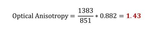
Therefore, the average optical anisotropy value for the aligned s-SWCNTs is ≈22 and for randomly oriented s-SWCNTs is ≈1.4.
Orientation Image in Figure 5
The V_V and H_H polarization images were exported from OMNICxi as grayscale TIFF images having the same intensity scale. This preserved the relative numerical values of each pixel between the two images. The TIFF images were imported into ImageJ where the subsequent orientation image was created by dividing the V_V image by the H_H image (3). The resulting image was scaled by a factor of 0.882 to correct for the lower instrument throughput caused by additional polarization optics (half wave plate) when collecting the H_H image.
References
- A. Mashal, D. Wieboldt, K. Jinkins, and M.S. Arnold, Spectroscopy31(s6), 36–44 (2016).
- Y. Joo, G. Brady, M. Arnold, and P. Gopalan, American Chemical Society, 3460–3466 (2014).
- J. Schindelin, et al., Nature Methods9(7), 676–682, PMID 22743772 (2012).


Getting accurate IR spectra on monolayer of molecules
April 18th 2024Creating uniform and repeatable monolayers is incredibly important for both scientific pursuits as well as the manufacturing of products in semiconductor, biotechnology, and. other industries. However, measuring monolayers and functionalized surfaces directly is. difficult, and many rely on a variety of characterization techniques that when used together can provide some degree of confidence. By combining non-contact atomic force microscopy (AFM) and IR spectroscopy, IR PiFM provides sensitive and accurate analysis of sub-monolayer of molecules without the concern of tip-sample cross contamination. Dr. Sung Park, Molecular Vista, joined Spectroscopy to provide insights on how IR PiFM can acquire IR signature of monolayer films due to its unique implementation.


AI-Based Neural Networks Revolutionize Infrared Spectra Analysis
May 13th 2024A Researcher from Lomonosov Moscow State University has developed a convolutional neural network (CNN) model for Fourier transform infrared (FT-IR) spectra recognition. This AI-based system is capable of classifying 17 functional groups and 72 coupling oscillations with remarkable accuracy, providing a significant boost to material analysis in fields like organic chemistry, materials science, and biology.

