|Articles|October 1, 2019
- Spectroscopy-10-01-2019
- Volume 34
- Issue 10
Adsorbate-Induced Morphological Changes of PVD-Deposited Nano Island Film SERS Substrates
Author(s)Daniel T Kwasnieski, Zachary D. Schultz
The morphology and gap spacing of nano-island film SERS substrates are key factors defining the properties of analyte‒substrate interactions. These results of the study described here have implications for understanding signal variation in SERS and in designing future SERS assays.
Advertisement
Thin films of noble metals deposited by physical vapor deposition (PVD) are a simple substrate commonly used in surface-enhanced spectroscopies. The morphology and gap spacing of these plasmonic substrates are key factors in the Raman enhancements observed from molecules in the optical near field. The nanometer gaps between nanostructured features of the substrate are associated with the strongest fields and the greatest enhancement of light-driven processes (scattering, absorption, fluorescence) that occur near the surface. Results shown here illustrate that chemical adsorbates and solvents interacting with the substrate can induce changes in the atomic, nanoscale, and mesoscale morphology of the plasmonic substrate, possibly leading to in situ species that play a role in the enhancement mechanisms associated with plasmonic nanostructures. In this work, we report on the morphology changes induced by functionalizing nano-island films (NIF) of silver and gold (film thickness = 4–30 nm) in thiol solutions (thiophenol and 1-hexanethiol). The adsorbate substrate interaction is hypothesized to cause aggregation or annealing-like surface rearrangements. NIF substrates of thickness <10 nm exhibit more significant changes than thicker films, as evidenced by SEM and UV-vis data. Insights into substrate design to account for analyte substrate interactions for surface enhanced Raman spectroscopy (SERS) are discussed in the context of strongly and weakly adsorbing analytes.
The enhancement of Raman scattering from molecules on the surface of plasmonic nanostructures (so-called surface–enhanced Raman scattering, or SERS) has been studied extensively for trace detection of analytes in a wide variety of applications (1–5). The localized surface plasmon resonance (LSPR) supported on nanostructured metal surfaces (the most commonly studied are silver, gold, and copper) under irradiation at optical frequencies is a result of the strong interaction between the conduction electrons confined in a sub-wavelength geometry and the incident electromagnetic wave. The oscillating electromagnetic field polarizes the electron cloud in the metal, and induces a resonant oscillation of the conduction electrons, giving rise to a new field concentrated around the nanostructure. Molecules within these enhanced fields exhibit increased Raman scattering. The strongest fields are found at the tip of nanoscale features with high aspect ratio or atomically sharp edges due to the "lightning rod effect," or in the nanometer gaps of neighboring nanoparticles, termed hotspots, due to field enhancements from interparticle coupling (6–9).
To capture these enhancements for trace chemical detection, considerable effort has been put into fabricating noble metal nanoparticle systems and studying their plasmonic properties. The structure, composition, and local dielectric environment of a plasmonic nanostructure influence the LSPR frequency and spatial intensity distribution of the excited field around the nanostructure. The choice of these parameters will vary depending on the application, and many fabrication methods have been developed to explore a vast design space for plasmonic substrates (10–12). These fabrication methods, ranging in complexity and performance, include nanolithography, physical vapor deposition (PVD), electrochemical roughening, colloidal nanoparticle immobilization, wet chemical reduction, and others.
One of the first-studied and simplest methods of preparing a SERS substrate is the physical vapor deposition of silver or gold onto a glassy substrate to produce nano-island films (NIFs). Within the category of PVD, films can be produced from sputtering, thermal evaporation, electron beam evaporation, and laser ablation, which largely exhibit similar properties. Thin films of these metals do not deposit conformally on smooth, glassy surfaces, due to low surface energy and poor wetting of the metal on the surface, but instead form isolated nanostructures with gaps between particles of the order of the particle diameter or smaller, thus facilitating plasmonic activity (13–19). The experimental parameters governing the resultant morphology of as-deposited films (and typical values found in the literature) are nominal film thickness (1-15 nm), deposition rate (0.001-0.1 nm/s), substrate temperature (100-500 °K), and vacuum pressure (<10-6 torr) (20-24). The morphology and optoelectronic properties of as–deposited films and those subject to various post-deposition treatments (thermal annealing [25-39], solvent annealing [31–35], chemical functionalization [21,31,36–46]) have been intensely investigated. The identity of the underlying substrate (glass [20–23, 25–27,31–40], quartz [42,45,46], calcium fluoride [16], silicon and geranium [28,41], formvar [47], and carbon [48,49]) and cleaning procedures also factor into the NIF morphology. For as–deposited films, the morphology is tunable from isolated ellipsoidal particles to randomly shaped particles coined nano-islands to semi-continuous film. Still, due to the random nature of the deposition process, nanoparticle size and shape distributions are rather broad, leading to some variation in the optical properties across the substrate. Above a certain thickness threshold (~20–30 nm), the film will become fully continuous and acquire a mirror-like appearance, and the plasmonic activity is significantly diminished as the average particle size is larger than the incident wavelength. Thick films (thickness >50 nm) can be prepared that display plasmonic activity given careful considerations of the deposition parameters, but these films will not be discussed here (50).
Although the physics giving rise to the enhanced electric fields is now well understood, SERS has been plagued by circumstances and effects that created a perception of irreproducibility. Some of this irreproducibility arises from large variations in the optical properties associated with differences in the nanostructure preparation. Other variations have been attributed to chemical effects, some of which date back to the initial discovery of SERS (51,52). It is also understood that changes in the nanostructures can alter the enhancements and, in some cases, quench the electric field (53).
The topic of this report is the much-studied thermally evaporated thin films of silver and gold (nominal film thickness <30 nm). The results of this work describe significant changes to the film morphology, and thus the corresponding optical properties, upon functionalization with self-assembled monolayers (SAMs) of thiols. Characterization by SEM and ultraviolet (UV)-vis spectroscopy indicates the formation of the thiol SAM perturbs the interparticle van der Waals forces, leading to a structural rearrangement of the film that mimics coalescence or aggregation of the nanoparticles. The observed structural rearrangement significantly alters the observed SERS enhancements.
Experimental
Nano-island Film Fabrication
Silver and gold NIF substrates were prepared by PVD. White glass microscope slides (Globe) were soaked in a Nochromix acid bath (Godax Laboratories) for >12 h. The slides were removed from the cleaning bath, rinsed thoroughly with ultrapure water (Thermo Fisher Scientific GenPure, 18.2 M⦠cm), and subsequently dried under nitrogen. The cleaned slides were loaded into the commercial PVD vacuum chamber (PVD Nano 36, Kurt J. Lesker Co.), the metal shot (silver, 99.999%, Sigma-Aldrich, and gold, 99.999%, Kurt J. Lesker Co.) to be resistively heated was placed in a tungsten boat, and the chamber was evacuated to a pressure of <10-6 torr. A quartz crystal microbalance (QCM) located near to the deposition surface monitored the deposition rate of the metal. During the deposition, the substrates were rotated at 10 rev/s. The pre-deposition procedure for heating the metal shot to the point of evaporation involved ramping the output power set point in two stages to ~80% and ~90% of the working deposition set point (ramp rate = 0.5 units/s, soak time = 45 s), after which a proportional-integral-derivatice (PID) rate control function was enabled to stabilize the rate at the working set point (rate = 0.003 nm/s). Then, the substrate shutter was opened to begin the deposition of metal onto the substrates, which proceeded until the nominal film thickness set point was reached as determined by the QCM (thickness = 4–30 nm). The temperature of the substrate was not monitored during the deposition.
Substrate Functionalization
Self-assembled monolayers of thiol (benzenethiol, benzene thiol [BT], Sigma-Aldrich, 99.9%; 1-hexanethiol, hydroxytryptophan [HT], Sigma-Aldrich, 95%; chemicals used as received) were deposited onto the as-prepared nano-island films by two methods: (1) soaking in a 10 mM ethanolic solution of the respective thiol for >12 h, after which the films were rinsed with ethanol for 10 s and subsequently dried under nitrogen. To study the impact of thiol concentration, some films were soaked in lower concentration BT solutions: 5 nM, 50 nM, 1 µM, and 50 µM; (2) positioning the substrate above a 10 µL droplet of the respective thiol inside a closed container to expose the surface to thiol vapor for 1 h; after removal no further treatment was performed.
UV-visible Spectroscopy
UV-vis transmission measurements of the thin film substrates were carried out by placing the substrate into the optical path of a VWR UV-1600PC spectrophotometer just in front of the sample cuvette holder that could not be modified to fit the microscope slides or cover slips. A blank slide or cover slip was used to obtain baseline reference spectrum. The extinction spectra were recorded using scan rate of 1 nm/s. The data were analyzed in MATLAB to determine LSPR wavelength and extinction maxima.
Raman Spectroscopy
Raman measurements were collected using a Renishaw inVia Raman microscope. The Renishaw mapping software was used to raster over approximately 20 µm × 20 µm areas, collecting a spectrum every 3 µm; the mapped areas varied from sample to sample but at least 50 spectra were recorded per map. The acquisition time was 1 s, and the microscope objective used had a 50x magnification and a numerical aperture (NA) of 0.75 (Olympus). The excitation power and laser was ~1 mW from a 632.8 nm HeNe laser (Thorlabs). The spectral windows collected for BT and HT were 700-1275 and 800-1350 cm-1 Raman shift, respectively. The data was analyzed using MATLAB and an open-source peak-fitting routine (54) to calculate peak areas based on Gaussian fits. The number of Gaussian line shapes included in the fit was 3 for BT and 1 for HT for the selected spectral windows 900-1200, and 1080-1140 cm-1 Raman shift, respectively. A linear baseline was subtracted from the spectrum before fitting to the Gaussian line shape.
Scanning Electron Microscopy
The nanoscale morphology of thin film substrates was characterized by imaging in the field emission mode of a FEI Apreo LoVac SEM. Imaging conditions were 1-2 kV, 6.3 pA, working distance 3-4 mm, stage bias -4000 V. The in-lens T1 component of the Trinity suite backscatter detectors of the SEM was used to acquire the signal.
Results
Figure 1 shows scanning electron micrographs of the silver NIFs obtained from different deposition thicknesses before and after functionalization with thiol. Isolated nanoparticles were observed in the 6 and 8 nm films (nominal film thickness measured during the deposition by QCM) that were roughly ellipsoidal, while a more heterogeneous mixture of shapes was found for the 14 nm film. After functionalization with thiols by soaking in ethanolic solutions, the observed particles appear closer together, suggesting smaller gap sizes between the islands formed.
Figure 1: Scanning electron micrographs of silver nano-island films, demonstrating morphological changes upon functionalization. Images (a) and (b) correspond to two different 6 nm samples, and (b) was functionalized with benzene thiols (BT). Images (c) and (d) correspond to a 8 nm sample that was imaged before and after functionalization with BT. The scale bar for the inset image in (d) is 1 µm. Images (e) and (f) correspond to different 14 nm samples, (f) was functionalized with HT.
This change in spacing is apparent upon visual inspection. Figure 2 shows the color of the films are also observed to change in different chemical environments. In Figure 2, the pristine NIF is observed to have a yellow hue. The extinction max of the pristine film is observed at 470 nm. When immersing the film in ethanol, a slight discoloration is observed and a shift in the extinction maxima to 490 nm is measured. When the films are allowed to dry over the course of a day, the change observed from exposure to ethanol is observed to be reversible, with the LSPR returning to near the same value as observed from the pristine film. However, upon functionalization with BT, a dramatic color change is observed visually that corresponds to change in the extinction maxima to 665 nm. The measured extinction spectrum is consistent with coupled or aggregated nanoparticles reported in the literature (55–57).
Figure 2: Color changes in the NIF are observed when exposed to different chemicals. (a) Photograph of colored silver 8 nm films diced from the same microscope slide at different stages of treatment (wavelength of extinction maximum indicated). (Left) The as-prepared film appears yellow colored to the eye. (Center) After soaking for 12 h in ethanol and drying under nitrogen, the film exhibits a slight discoloration. The appearance nearly returns to the as-prepared state over the course of a day. (Right) After soaking for 12 h in BT, the film becomes blue-colored, and the change is permanent. All samples exhibit small shifts in color over the course of a week when exposed to ambient atmosphere. (b) UV-vis spectra of the silver 8 nm films from (a).
The data in Figures 1 and 2 suggest a significant change in the NIFs upon adsorption of BT. To understand this effect, we investigated how different deposition conditions and functionalization concentrations affect the change in optical properties. Figure 3 shows that the single peak observed in the extinction spectrum broadens and red-shifts as the thickness of the metal deposition increases. Wavelength (Figure 3b) and peak absorbance value (Figure 3c) are shown to increase with film thickness. Similar trends were observed for both silver and gold films. The observed trends agree with previous reports of changes in the LSPR of NIFs with changes in deposition thickness (15,17,22,23).
Figure 3: UV-vis characterization of NIF. (a) UV-vis extinction spectra acquired in transmission mode of silver (Ag) films of thickness = 2, 6, 8, 10, 12, 14, and 20 nm, indicating general trends of increased extinction, peak broadening, and a red shift of the LSPR wavelength for thicker films. (b) Plot of LSPR peak wavelength, and (c) extinction for silver (Ag) (black circles) and gold (Au) (red squares) films of various nominal thickness.
The broadening of the extinction spectrum with increasing nominal film thickness shown in Figure 3a is commonly observed as films transition from nanomaterials to mesoscale materials (15,17,19,26). At a deposition thickness of 20 nm, the width of the feature in the extinction spectrum is consistent with a heterogeneous collection of particles with varying shapes and sizes. Analysis of extinction spectra obtained from multiple films indicates that above a deposition of 15 nm, the nano-islands percolate into larger structures; this increased interconnectedness has been observed in this regime of film thickness (15,17,26). The trends in the extinction spectra agree with the observations from the electron micrographs (Figure 1). Increased film thickness gives rise to a larger size nanoparticle consistent with increased and red-shifted extinction.
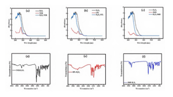
Figure 4 illustrates the changes in extinction spectrum observed from different deposition thicknesses after functionalization with either BT or HT. In all cases, a marked change in the extinction spectrum is observed as the thiols adsorb onto the NIFs. It is well understood that the change in the dielectric environment will shift the frequency of the LSPR (the basis of surface plasmon resonance sensing [10,42,44]). The change in line shape observed from smaller thickness films (Figures 4a, b, and d, thickness < 10 nm) show splitting more consistent with plasmon hybridization from the aggregation of discrete particles. At thicker depositions (Figure 4c, 14 nm), the change in the extinction spectrum is best described by a shift in frequency but not line shape. The changes in line shape for the different thickness film is observed from both solution and gas phase adsorption (data not shown) of the thiols onto the NIFs. This indicates that the deposition thickness influences the morphological and optical changes resulting from molecular adsorption, but that adsorption is a key event.
Figure 4: Characterization of NIF LSPR by UV-vis before and after functionalization. Spectra of silver (Ag) and gold (Au) films of thickness (a) Ag 6 nm, (b) Ag 8 nm, (c) Ag 14 nm, and (d) Au 4 nm. Solid curves correspond to measurements of as-prepared films, dash-dotted curves correspond to the same film after soaking in a 10 mM ethanolic thiol solution overnight (black = BT, red = HT).
Given the known relationship between nanostructure and the plasmonic fields responsible for surface-enhancement effects, we sought to understand the impact of this adsorption-driven change in film structure on the observed SERS signals.
Figure 5 plots the results obtained from the Raman mapping experiments of BT and HT-functionalized films. SERS spectra of the two molecules are shown in Figure 5b, demonstrating that BT has a much larger Raman cross-section compared to HT. A representative map analysis of a silver 8 nm NIF functionalized with BT is displayed in Figure 5a and 5c. In general, the SERS response from similarly prepared films is quite reproducible. In the map shown, the step size of approximately 3 µm, which is larger than the laser spot size (diffraction limited at approximately 500 nm), ensures that each spectrum is obtained without possible photodamage from the previous acquisition. With a 1 s integration, a large signal of approximately 30,000 counts is observed. The spectra show excellent signal-to-noise ratios. When examining the variation in intensity across the silver NIF substrate, the peak area of the 1000 cm-1 band in BT changes by about 15% from the brightest to dimmest spectra.
Figure 5: SERS mapping of silver 8 nm NIF functionalized with BT. (a) Optical image of the mapped area at 50x magnification. (b) Representative SERS spectrum of BT (black) and HT (red). The bands marked with an asterisk are used for calculating the peak area from Gaussian fits in (d). (c) Colormap of the peak area of the 1000 cm-1 band of BT. The map was obtained by rastering in 3 µm steps, acquiring a spectrum at each pixel for 1 s (laser power = 0.7 mW). (d) Map-averaged peak area of the 1000 cm-1 band of BT (black) and the 1110 cm-1 band of HT (red) vs. nominal film thickness. Error bars indicate the standard deviation for a mapped area of 50-100 pixels.
Comparing across different films, the average SERS signal obtained from the NIF substrates shows little dependence on the deposition thickness below 15 nm (Figure 5d). Once the thickness of the deposited metal exceeds 15 nm, the SERS intensity is observed to decrease for both BT and HT. As discussed above, NIFs obtained from thicker depositions exhibit larger interconnected particles. These interconnected features decrease the density of hot spots (nanometer gaps between particles) and therefore these films exhibit less SERS. Beyond the change in observed SERS intensity with thicker deposits (thickness > 15 nm), the trends associated with the as-deposited film properties are less discernible. The correlation between the topography and SERS intensity suggests the reorganization is observed for smaller features and that once the as-deposited features coalesce into larger islands, the ability to reorganize and boost the SERS signal is diminished.
As noted above, the identity of the adsorbate influenced the reorganization of the nano-islands in the film, where ethanol did not produce the same effect as BT or HT. In Figure 6, we examined how the concentration of BT in solution alters the extinction (indicative of the island reorganization) and the observed SERS signal. In Figure 6a, the extinction is observed to remain largely unchanged at adsorbate concentrations below 50 µM (spectra for films soaked in 5 nM and 1 µM not shown). When a film was initially soaked at a 50 nM concentration of BT, the extinction was largely unchanged. Upon resoaking the same film in 10 mM of BT, the extinction was observed to change consistent with the reorganization of the NIFs described above. The observed change with re-soaking was the same as soaking a second pristine film in a 50 µM solution. This indicates that a critical coverage of BT (or other adsorbate) is necessary to induce the reorganization of the metal islands.
Figure 6: Characterization of BT-functionalized silver NIF at low soaking concentrations. (a) UV-vis transmission spectra series of two silver 8 nm samples after different BT treatment steps. (b) SERS spectra for four silver samples soaked in various concentrations of BT. SERS spectra were recorded with 633 nm laser excitation for 10 s at laser power 3, 0.6, 0.6, and 0.05 mW for the respective films. The inset magnifies the spectral region 950–1150 cm-1 where the prominent BT modes are present in the 5 nM, 50 nM, and 50 µM samples, but not the 1 µM sample.
In Figure 6b, the SERS spectrum observed from the NIFs is shown to change as function of adsorbate concentration. Solutions of BT below 1 µM did not evince a significant SERS signal, suggesting this concentration is below the limit of detection. Peaks are sporadically observed at frequencies consistent with BT, but do not increase appreciably in intensity until higher concentrations. At a 50 µM concentration of BT, a markedly different spectrum is observed. The peaks are observed with significantly greater intensity. The change in intensity at 50 µM is dramatically larger than the signals observed from 50 nM and 1 µM adsorbate concentrations. Additionally, the change in intensity correlates with a dramatic change in the extinction spectrum (Figure 6a) suggesting that this change in the spectrum is related to the reorganization of the NIFs.
Discussion
The characterization of silver and gold NIFs was accomplished with SEM, UV-vis, and SERS measurements. Our analysis of as-deposited films from our work agrees well with the literature with respect to the investigated deposition parameters (17,21–23,26,36). The plasmonic properties of these thin films are apparent upon visual inspection, since the films are colored and semi-transparent, as opposed to bulk metal. Similar to the Lycurgus cup, the films show differences in reflection and transmission (15,20). What has not been directly correlated in the literature is the increased SERS response that arises from the structural reorganization of the plasmonic metal islands and the analyte dependence of this effect.
Previous studies of the morphological and optical properties of PVD thin films suggest the NIFs can be characterized as oblate spheroids with an aspect ratio (R) between 0.1 and 0.5, reflecting the island diameters are ~2-10x their height (17). Thus, with sufficient interparticle spacing (greater than a few nanometers, as is the case for thicknesses <15 nm), the LSPR of NIFs is observed to be a single peak reflecting the in-plane mode along the major axis of the isolated ellipsoids. Changes in the LSPR have been described when the films are annealed, which causes a reorganization of the islands into larger, more spheroidal particles (17,25–30), and when molecular adsorption changes the dielectric environment of the film. A number of studies have noted the change in the local dielectric environment from adsorbates such as solvents (31–35), dye molecules (36–39), silanes (58), thiols (33,42–44,46), and others (21,31,45); however, a structural rearrangement has not been widely implicated (21,45–46). Indeed, to facilitate LSPR sensing, the substrates for the deposition of NIFs were pre-functionalized with mercaptopropyltrimethoxysilane (MPTS) to improve film stabilization (44). In that case, when the NIFs deposited on MPTS-treated glass were functionalized with a dithiol, only a small red-shift of the LSPR (< 50 nm) was observed, typical of a change in the local dielectric environment with increasing coverage (thickness) of the adsorbed layer. This change indicates stabilized films provide morphological stability which may impact utility as SERS sensors. On the other hand, structural rearrangements of NIF on unmodified quartz substrates were described upon functionalization with two different molecules by measurements of the LSPR and atomic force microscopy (45,46).
The change in morphology we claim suggests that intermolecular forces, such as increased van der Waals forces, between the nano-islands can drive aggregation. The change in the intermolecular forces derives from the coverage of the adsorbate and produces a marked change in the observed SERS signal. While not a classical "chemical effect," here the electromagnetic enhancement clearly derives from chemical functionalization, in this case changing the spacing and the local electric fields experienced by the adsorbate. Indeed, there are now SERS substrates commercially available that take advantage of this effect, using molecular adsorption to pull nano-pillars together (Silmeco, reference [59]). Our results illustrate how these aggregation affects alter the observed signals and likely affect selectivity for different analytes. Ethanol did not drive rearrangement in the same manner as the alkane thiols. There is clearly a balance between coverage and chemical properties of the adsorbate that drive the rearrangement. The changes we report in the UV-vis spectrum provide an easy experiment to assess if these effects are involved in experiments with other adsorbates and applications. Understanding these effects may enable selective sensors for future applications.
Conclusion
We have shown that molecular adsorption can drive structural rearrangements in silver and gold NIFs commonly used as SERS substrates. Adsorption of a significant portion of a monolayer changes the structure of small NIFs, typically derived from deposition thicknesses less than 15 nm, that are evident in SEM, UV-vis, and SERS measurements. At low analyte coverages, the SERS spectrum is significantly weaker and does not change with concentration, suggesting stochastic effects. Above a critical coverage, changes are observed that correlated with SEM and UV-vis measurements to suggest the nano-islands are closer and coupling more strongly. These results have implications for understanding signal variation in SERS and in designing future SERS assays.
Acknowledgments
This work was supported by National Science Foundation awards CHE-1830994 and DBI-1830153 and funding from the Ohio State University. Electron microscopy was performed at the Center for Electron Microscopy and Analysis (CEMAS) at The Ohio State University.
References
(1) P. L. Stiles, J. A. Dieringer, N. C. Shah, R. P. Van Duyne, Annu. Rev. Anal. Chem. 1, 601–626 (2008).
(2) N. J. Halas, S. Lal, W. S. Chang, S. Link, P. Nordlander, Chem. Rev. 111(6), 3913–3961 (2011).
(3) A. H. Nguyen, E. A. Shangle, and Z. D. Schultz, Rev. Anal. Chem. 36(4), 20160037 (2017).
(4) F. Sun, D. D. Galvan, P. Jain, Q. Yu, Chem. Comm. 53, 4550–4561 (2017).
(5) F. Wang, S. Cao, R. Yan, Z. Wang, D. Wang, H. Yang, Sensors 17, 2689 (2017).
(6) A. Otto, J. Raman Spectrosc.37, 937–947 (2006).
(7) E. C. Le Ru, M. Meyer, E. Blackie, P. G. Etchegoin, J. Raman Spectrosc. 39, 1127–1134 (2008).
(8) K. L. Wustholz, A. I. Henry, J. M. McMahon, R. G. Freeman, N. Valley, M. E. Piotti, M. J. Natan, G. C. Schatz, and R. P. Van Duyne, J. Am. Chem. Soc. 132(31), 10903–10910 (2010).
(9) K. D. Alexander, K. Skinner, S. Zhang, H. Wei, and R. Lopez, Nano Lett. 10, 4488–4493 (2010).
(10) Y.-S. Shon, H. Y. Choi, M. S. Guerrero, and C. Kwon, Plasmonics 4, 95–105 (2009).
(11) M. Fan, G. F. S. Andrade, and A. G. Brolo, Anal. Chim. Acta 693(1-2), 7–25 (2011).
(12) I. Abdulhalim, Small10(17), 3499–3514 (2014).
(13) T. H. Wood and M. V. Klein, Solid State Commun. 35(3),263–265 (1980).
(14) G. S. A. Shawki, M. G. El-Sherbiny, and F. B. Salem, Thin Solid Films 75(1), 29–36.(1981).
(15) C. A. Davis, D. R. McKenzie, and R. C. McPhedran, Opt. Comm. 85(1), 70–82 (1991).
(16) P. Dawson, K. B. Alexander, J. R. Thompson, J. W. Haas III, and T. L. Ferrell, Phys. Rev. B 44(12), 6372–6381 (1991).
(17) R. P. Van Duyne, J. C. Hulteen, and D. A. Treichel, J. Chem. Phys. 99(3), 2101–2115 (1993).
(18) U. K. Chettiar, P. Nyga, M. D. Thoreson, A. V. Kildishev, V. P. Drachev, and V. M. Shalaev, Appl. Phys. B: Lasers Opt. 100(1), 159–168 (2010).
(19) G. Santoro, S. Yu, M. Schwartzkopf, P. Zhang, S. Koyiloth Vayalil, J. F. H. Risch, M. A. Rübhausen, M. Hernández, C. Domingo, and S. V. Roth, Appl. Phys. Lett. 104(24), 243107 (2014).
(20) J. G. Bergman, D. S. Chemla, P. F. Liao, A. M. Glass, A. Pinczuk, R. M. Hart, and D. H. Olson, Opt. Lett. 6(1), 33–35 (1981).
(21) V. L. Schlegel and T. M. Cotton, Anal. Chem. 63(3), 241–247 (1991).
(22) W. A. Weimer and M. J. Dyer. Appl. Phys. Lett. 79(19), 3164–3166 (2001).
(23) R. Gupta, M. J. Dyer, and W. A. Weimer, J. Appl. Phys. 92(9), 5264–5271 (2002).
(24) K. M. McPeak, S. V. Jayanti, S. J. P. Kress, S. Meyer, S. Iotti, A. Rossinelli, and D. J. Norris, ACS Photonics 2(3), 326-333 (2015).
(25) G. Kalyuzhny, A. Vaskevich, G. Ashkenasy, A. Shanzer, and I. Rubinstein, J. Phys. Chem. B 104(34) 8238–8244 (2000).
(26) I. Doron-Mor, Z. Barkay, N. Filip-Granit, A. Vaskevich, and I. Rubinstein, Chem. Mater. 16(18), 3476–3483 (2004).
(27) P. Cheng, D. Li, and D. Yang, Optoelectron. Adv. Mater., Rapid Commun. 5(4), 455–458 (2011).
(28) E. Thouti, N. Chander, V. Dutta, and V. K. Komarala, J. Opt. 15(3), 035005 (2013).
(29) M. G. Sreenivasan, S. Malik, S. Thigulla, and B. R. Mehta, J. Nanomater. 2013, 247045 (2013). doi:10.1155/2013/247045.
(30) X. Sun and H. Li, Nanotechnology 24, 355706 (2014).
(31) S. E. Roark and K. L. Rowlen, Anal. Chem. 66(2), 261–270 (1994).
(32) S. E. Roark, D. J. Semin, A. Lo, R. T. Skodje, and K. L. Rowlen, Anal. Chim. Acta 307(2-3), 341–353 (1995).
(33) M. D. Malinsky, K. L. Kelly, G. C. Schatz, and R. P. Van Duyne, J. Am. Chem. Soc. 123(7), 1471–1482 (2001).
(34) Y. Luo, J. Ruff, R. Ray, Y. Gu, H. J. Ploehn, and W. A. Scrivens, Chem. Mater. 17(20), 5014–5023 (2005).
(35) X. Li, W. Xu, H. Jia, X. Wang, B. Zhao, B. Li, and Y. Ozaki, Thin Solid Films 474(1-2), 181–185 (2005).
(36) A. M. Glass, P. F. Liao, J. G. Bergman, D. H. Olson, Opt. Lett. 5(9), 368–370 (1980).
(37) S. Garoff, D. A. Weitz, T. J. Gramila, C. D. Hanson, Opt. Lett. 6(5), 245–247 (1981).
(38) S. Garoff, R. B. Stephens, C. D. Hanson, and G. K. Sorenson, Opt. Comm. 41(4), 257–262 (1982).
(39) D. A. Weitz, S. Garoff, J. I. Gersten, and A. Nitzan, J. Chem. Phys. 78(9), 5324–5338 (1983).
(40) C. A. Murray and S. Bodoff, J. Chem. Phys. 85(1), 573–584 (1986).
(41) J. P. Goudonnet, J. L. Bijeon, R. J. Warmack, and T. L. Ferrell, Phys. Rev. B 43(6), 4605–4612 (1991).
(42) G. Kalyuzhny, M. A. Schneeweiss, A. Shanzer, A. Vaskevich, I. Rubinstein, J. Am. Chem. Soc. 123(13), 3177-3178 (2001).
(43) Q. Ye, J. Fang, and L. Sun, J. Phys. Chem. B 101(41), 8221–8224 (2002).
(44) I. Doron-Mor, H. Cohen, Z. Barkay, A. Shanzer, A. Vaskevich, and I. Rubinstein, Chem. Eur. J. 11(19), 5555–5562 (2005).
(45) T. Del Rosso, E. Giorgetti, S. Cicchi, M. Muniz-Miranda G. Margheri, A. Giusti, A. Rindi, G. Ghini, S. Sottini, A. Marcelli, P. Foggi, J. Lumin. 129(12), 1955–1959 (2009).
(46) M. Muniz-Miranda, T. Del Rosso, E. Giorgetti, G. Margheri, G. Ghini, S. Cicchi, Anal. Bioanal. Chem. 400(2), 361–367 (2011).
(47) R. S. Sennett and G. D. Scott, J. Opt. Soc. Am. 40(4), 203–211 (2008).
(48) H. Ishida, H. Fukuda, G. Katagiri, and A. Ishitani, Appl. Spectrosc. 40(3), 323–330 (1986).
(49) A. Urich, A. Pospischil, M. M. Furchi, D. Dietze, K. Unterrainer, and T. Mueller, Appl. Phys. Lett. 101(15), 153113 (2012).
(50) M. Levlin, A. Laakso, H.E.-M. Niemi, and P. Hautojarvi, Appl. Surf. Sci. 115(1), 31–38 (1997).
(51) M. G. Albrecht and J. A. Creighton, J. Am. Chem. Soc. 99(15), 5215–5217 (1977).
(52) I. Mrozek and A. Otto, Europhys. Lett. 11(3), 243–248 (1990).
(53) W. Zhu and K. B. Crozier, Nature Comm. 5, 5228 (2014).
(54) T. O'Haver, Interactive Peak Fitter 9.2, Mathworks, Natick, MA, 2013.
(55) E. Prodan, C. Radloff, N. J. Halas, and P. Nordlander, Science 302(5644), 419–422 (2003).
(56) D. W. Brandl, N. A. Mirin, and P. Nordlander, J. Phys. Chem. B 110(25), 12302–12310 (2006).
(57) P. K. Jain and M. A. El-Sayed, Chem. Phys. Lett. 487(4-6), 153–164 (2010).
(58) I. Ruach-Nir, T.A. Bendikov, I. Doron-Mor, Z. Barkay, A. Vaskevich, and I. Rubinstein, J. Am. Chem. Soc. 129(1), 84–92 (2007).
(59) M. S. Schmidt, J. Hübner, and A. Boisen, Adv. Mater. 24(10), 11-18 (2012).
Daniel T. Kwasnieski and Zachary D. Schultz are with the Department of Chemistry and Biochemistry at The Ohio State University, in Columbus, Ohio. Direct correspondence to:
Articles in this issue
over 6 years ago
Using Reference Materials, Part II: Photometric Standardsover 6 years ago
Detecting and Identifying Food Colorants with SERSover 6 years ago
The 2019 Emerging Leader in Molecular Spectroscopy Awardover 6 years ago
Vol 34 No 10 Spectroscopy October 2019 Regular Issue PDFAdvertisement
Related Content
Advertisement
![Figure 3: Plots of lg[(F0-F)/F] vs. lg[Q] of ZNF191(243-368) by DNA.](https://cdn.sanity.io/images/0vv8moc6/spectroscopy/a1aa032a5c8b165ac1a84e997ece7c4311d5322d-620x432.png?w=350&fit=crop&auto=format)

Advertisement
Advertisement
Trending on Spectroscopy Online
1
Where is Raman Spectroscopy Delivering the Most Value for Real-Time Chemical Analysis in Oil and Gas?
2
Fujifilm, Horiba Unveil New Inline Raman System
3
Best of the Week: Prebiotic Chemistry, Real-Time Chemical Analysis, Previewing ISMS 2026
4
Tips for Young Researchers Attending ISMS 2026 Next Week
5