
News|Articles|February 11, 2026
Hybrid QCL–Silicon Platforms Advancing Mid-Infrared Photonics
Author(s)Alexis Hobl, Will Wetzel
Listen
0:00 / 0:00
Key Takeaways
- Heterogeneous MIR integration is shifting emphasis from standalone devices to manufacturable photonic systems constrained by coupling tolerances, thermal management, yield, and packaging workflows.
- Efficient III–V-to-silicon optical coupling, cavity partitioning for stable single-mode emission, and robust current/heat handling remain primary integration barriers for QCL-on-silicon platforms.
In an interview recapping the Photonics West Conference, which took place in San Francisco, California in January, Alexis Hobl of CEA-Leti sat down with Spectroscopy to discuss his work integrating quantum cascade lasers (QCLs) with silicon photonic platforms and how it is evolving mid-infrared (MIR) photonics.
Advertisement
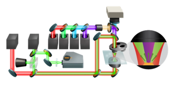
The SPIE Photonics West Conference took place in San Francisco, California from January 16–21, 2026 (1). Over the course of the conference, numerous talks took place that highlighted the latest trends and developments in optics and photonics. One of those discussions, presented by Alexis Hobl of CEA-Leti, highlighted how integrating quantum cascade lasers (QCLs) with silicon photonic platforms is transforming mid-infrared (MIR) photonics by enabling compact, scalable, and complementary metal-oxide-semiconductor (CMOS)-compatible devices (2). In his presentation, Hobl reflected on the recent progress made building three hybrid III–V/Si QCL architectures, which included distributed feedback (DFB), distributed Bragg reflector (DBR), and ultra-compact designs using diffractive photonic crystals and refractive micro-ring cavities (2). Each architecture was optimized for efficient MIR emission and seamless silicon integration (2).
As a follow-up to his lecture at the conference, Spectroscopy sat down with Hobl to discuss these advances more at length.
I’d like to start off this interview by asking about your experience at the Photonics West Conference. What was it like to be on the ground there, and were there any talks that stood out to you?
Photonics West was intense in the best way. The pace was fast, the audience was very broad (from fundamental photonics to industrial roadmaps), and you immediately felt what topics are maturing because people from different communities start using the same vocabulary—packaging, yield, scalability, and system-level validation. For me, it was particularly valuable to see MIR photonics increasingly discussed not only as devices, but as integrated systems.
A few themes that stood out were the push toward heterogeneous integration (especially where the photonic platform is no longer just routing light, but shaping the cavity and the functionality), and the growing focus on realistic manufacturability constraints—thermal management, coupling tolerances, wafer-scale reproducibility, and packaging. It also struck me how much attention is moving toward “What can you integrate next to the source?” (filters, interferometers, multiplexers, sensing readout), because that’s where silicon photonics really changes the game.
Beyond our QCL work, it was also great to see CEA-Leti presenting other system-level integration approaches at Photonics West as well, such as co-packaged microLED and organic photodetector architectures enabling display-integrated optical sensing.
What are the key challenges in integrating QCLs with silicon-based photonic platforms, and how are recent hybrid III–V/Si architectures addressing these obstacles?
Integrating QCLs with silicon-based photonics is challenging because you’re trying to connect two worlds that are optimized for different things.
The first challenge is efficient optical coupling. You need to transfer power from a III–V active region into a silicon waveguide with low loss, while keeping the mode well controlled. The second challenge is spectral control and cavity engineering. QCLs need robust feedback and stable single-mode operation. Doing that in a hybrid environment requires careful design partitioning between III–V gain and silicon photonic functions. The third challenge is thermal and electrical management because QCL performance is highly sensitive to temperature and current injection conditions. Finally, there’s fabrication robustness challenges, which includes alignment tolerances, bonding and integration repeatability, and the ability to scale beyond single-lab prototypes.
Recent hybrid III–V/Si architectures address these obstacles by using silicon photonics not just as a passive waveguide layer, but as an active cavity and feedback toolbox. In our work, we highlighted three complementary approaches: (i) adiabatic coupling into a phase-matched silicon platform for robust power transfer and single-mode emission; (ii) external silicon DBR cavities where the feedback is implemented in silicon for flexibility and control; and (iii) ultra-compact micro-source concepts (photonic crystals/micro-rings) that exploit strong confinement and resonance to shrink footprint dramatically.
How do the DFB, DBR, and photonic-crystal/micro-ring–based QCL designs differ in terms of emission efficiency, footprint, and integration complexity for MIR applications?
These architectures differ mainly in where you place the “functions”: gain, feedback, wavelength selection, and out-coupling.
Hybrid DFB QCL (with adiabatic coupling on SONOI)
- Emission efficiency / usefulness: very robust single-mode behavior with efficient transfer into silicon waveguides, which is ideal when you want to feed a photonic circuit reliably.
- Footprint: moderate—still compact, but not “micro-source” scale (1 mm 2 mm).
- Integration complexity: the key is precise mode matching and adiabatic transition design; once that is robust, it becomes a strong candidate for scalable PIC integration.
Hybrid QCL with external silicon DBR cavity
- Emission efficiency/usefulness: strong in terms of spectral control and potential tunability because feedback is engineered in silicon; the gain section can be decoupled from the reflector design.
- Footprint: typically larger than micro-sources because of DBR sections, but can enable extra functions (filters, reflectors, tuning) within the same platform.
- Integration complexity: higher at the system level, but extremely attractive architecturally because silicon gives you more degrees of freedom for cavity design and multifunctionality.
Photonic crystal/micro-ring micro-sources
- Emission efficiency/usefulness: designed for extreme compactness; the physics relies on strong optical confinement and resonant effects, with possibilities like surface emission and low threshold in very small cavities.
- Footprint: the smallest—sub-100 µm scale concepts are the real differentiator here.
- Integration complexity: can be demanding in nanofabrication and tolerance control, but the payoff is dense on-chip integration and potentially new architectures not feasible with conventional ridge lasers.
What advantages does silicon photonics offer for MIR QCL devices compared with traditional III–V-only platforms?
Silicon photonics brings a platform mindset. This means there is high-index-contrast routing, compact passive components, and mature design methodologies for building circuits, not just lasers.
Compared to III–V-only approaches, silicon-based photonics can offer the following:
- Scalable integration of functions (filters, splitters, interferometers, multiplexers) next to the laser, enabling system-level PICs rather than discrete assemblies.
- Cavity engineering flexibility because you can implement parts of the feedback and wavelength control in silicon (for example, DBR structures), opening paths to tunability and multifunctionality.
- Compactness and repeatability, especially when high-contrast waveguides allow small bend radii and dense layouts.
- A clearer route toward wafer-scale co-integration, where the source and photonic circuit are designed together.
How might compact, CMOS-compatible QCL systems influence future developments in spectroscopy and sensing, particularly in environmental, biomedical, or defense-related applications?
If you can make QCL-based MIR systems compact and integration-friendly, you shift MIR spectroscopy from “specialized instruments” toward deployable sensing modules. For environmental monitoring, smaller, more robust MIR sources can enable distributed sensing (industrial sites, indoor air quality, leak detection) with strong molecular selectivity. In the biomedical industry, MIR is powerful for chemical fingerprinting. Integrated sources could help move toward portable diagnostics or lab-on-chip style analyzers, where stability and alignment-free operation matter a lot. And in defense-related applications, compact MIR sources are relevant for stand-off detection, chemical agent sensing, and robust field instrumentation where size, weight, power, and reliability dominate.
The real transformation comes when the laser is no longer “the big separate box,” but instead a building block inside a photonic system with on-chip routing, filtering, and potentially integrated detection.
Looking ahead, what breakthroughs or engineering innovations are still needed to achieve fully scalable and manufacturable MIR photonic systems based on hybrid QCL–silicon architectures?
The path to manufacturable hybrid MIR systems is becoming clearer, but a few engineering breakthroughs still matter a lot. For instance, higher and more tolerant coupling efficiency is needed to improve the adiabatic couplers and mode converters, so performance is robust against process variations. Second, QCLs are unforgiving thermally, so scalable architectures need excellent heat extraction and stable injection schemes compatible with integration constraints. Third, we need to integrate additional photonic functions that can unlock system value, which would require seamless co-integration of multiplexers, filters, interferometers, and signal conditioning circuits next to the source. Fourth, DBR-based concepts are promising for tunability and spectral agility, so practical tuning mechanisms and stable control loops will be key. And finally, we’ll need wafer-scale reproducibility and packaging. Demonstrating repeatability across many devices and moving toward packaging flows that preserve MIR optical performance is essential for translation beyond the laboratory.
References
- SPIE, SPIE Photonics West. SPIE.org. Available at:
https://spie.org/conferences-and-exhibitions/photonics-west (accessed 2026-01-27). - Hobl, A. Advanced Architectures for Hybrid III-V/Silicon Quantum Cascade Lasers: Toward Integrated Mid-infrared Photonic Platforms. Presented at the SPIE Photonics West Conference, in San Francisco, California on January 19, 2026. Available at:
https://spie.org/photonics-west/presentation/Advanced-architectures-for-hybrid-III-V-silicon-quantum-cascade-lasers/13902-2
Advertisement
Related Content
Advertisement


Advertisement
Advertisement
Trending on Spectroscopy Online
1
X-Ray Spectroscopy Analysis: Techniques and Applications Across Science and Industry
2
Educating Students on Spectroscopy
3
Submicron IR Detects and Localizes Microplastics in Biological Samples
4
Reading the Heat of the Giza Pyramids with Infrared Thermography
5