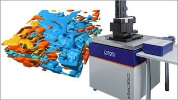
Hybrid Wafer Metrology for Bump Inspection and Overlay Control in Semiconductor Device Manufacturing
Monday, November 14th, 2022 at 11am EST|8am PST|6pm IST Join us for this web seminar to learn about advanced hybrid metrology to optimize semiconductor R&D and high-volume manufacturing processes, including bump inspection in thin-film analysis, and thickness and composition measurements of AgSn micro solder bumps using a monochromatic micro X-ray beam.
Register Free:
Event Overview:
Advanced Wafer Metrology efficient approach from FEOL through WLP, leading to in-line solutions to automate and optimize semiconductor manufacturing processes. Hybrid Metrology combines XRF measures elemental composition and film thickness, a 2D Microscope used for pattern recognition, CD calculation, 3D Scanner height measurement, area scan, wafer surface roughness, and bumps co-planarity.
Multi-sensor technology combined with integrated software leads the path of Inspection and metrology of 3D structures, thin films, multi-film stacks, and organic applications of the semiconductor industry.
Hybrid Metrology enables advanced metrology as an integrated part of the fab process, from FEOL through WLP. High-volume chips and semiconductor manufacturers demand automated high-throughput instruments, thickness and composition measurements, low-contamination wafer handling, and pattern recognition-based position control; to guarantee high-reliability machine performance and low power consumption and cost of ownership.
The increasing demands of materials and geometries in modern Semiconductor and Micro-Electronic manufacturing to deliver a non-destructive metrology and inspection tool that preserves the inspected elements with cutting-edge technology, monochromatic optics, polychromatic optics, and beam size.
Key Learning Objectives:
· Understanding bump Inspection in Thin films
· Implementation of Monochromatic Micro X-ray Beam for effective thickness and composition measurements of AgSn Micro Solder Bump
· Elemental analysis and detection of PD measurement on GaAs wafer
· Tool Configuration for bumps and copper pillars inspection
· Measure single-solder bumps as small as 10 μm diameter
· Inspect a range of parameters: across the wafer, wafer-to-wafer, and lot-to-lot
· Measure CD and the total height of single bumps using a 2D microscope, 3D scanner
Speakers:
Avishai Shklar
CTO - Chief Technology Officer
Rigaku XwinSysvine
Avishai Shklar has worked in the Semiconductor industry for 25+ years, gaining experience in Semiconductor metrology tools. As the Chief Technology Officer for Rigaku XwinSys, Avishai is passionate about advanced imaging tools for wafer inspection and metrology. Graduated as an Electronic Engineer from the Technion–Israel Institute of technology, and received an MBA from the Netanya Academic College. He was recognized for his fine pitch bonding tool for constrained bonding tool patents.
Boris Fridman
Application Team Manager
Rigaku XwinSys
Boris Fridman graduated from the Technion–Israel Institute of Technology Bachelor of Science in Physics and has been successful as an Applications Engineer for Nikkon, Systems Engineer for KLA, and an Application & Systems Engineer Manager for Rigaku Xwinsys.
Idan Raiter
Application Team Manager
Rigaku XwinSys
Idan Raiter has been a successful research assistant at the nanocrystals laboratory of semiconductors a the Technion–Israel Institute of Technology, an the Applications Team leader for Xemetrix, and the Applications Team Manager for Rigaku Xwinsys. He graduated from the Technion– Israel Institute of Technology with a Bachelor’s Degree in Biochemical Engineering. He has been recognized for his work on synthesis and optical characterization of semiconductors quantum dots.
Times and Dates:
Monday, November 14th, 2022 at 11am EST|8am PST|6pm IST
Sponsor:
Rigaku
Register Free:
Newsletter
Get essential updates on the latest spectroscopy technologies, regulatory standards, and best practices—subscribe today to Spectroscopy.


