Article
Spectroscopy
Spectroscopy
Agilent Technologies, Inc.
Agilent Technologies Inc. (NYSE: A), a global leader in life sciences, diagnostics and applied chemical markets, is the premier laboratory partner for a better world. Agilent works with customers in more than 100 countries, providing instruments, software, services, and consumables for the entire laboratory workflow.
Company Description
Agilent Technologies Inc. (NYSE: A), a global leader in life sciences, diagnostics and applied chemical markets, is the premier laboratory partner for a better world. Agilent works with customers in more than 100 countries, providing instruments, software, services, and consumables for the entire laboratory workflow. Agilent generated revenues of $4.04 billion in fiscal 2014. The company employs about 12,000 people worldwide. Information about Agilent is available at www.agilent.com.

Chief Spectroscopic Techniques Supported
- Food safety and quality
- Environmental testing
- Energy/petrochemical
- Forensics
- Pharmaceutical
- Drug discovery
- Materials testing & research
- Geochemistry, mining & metals
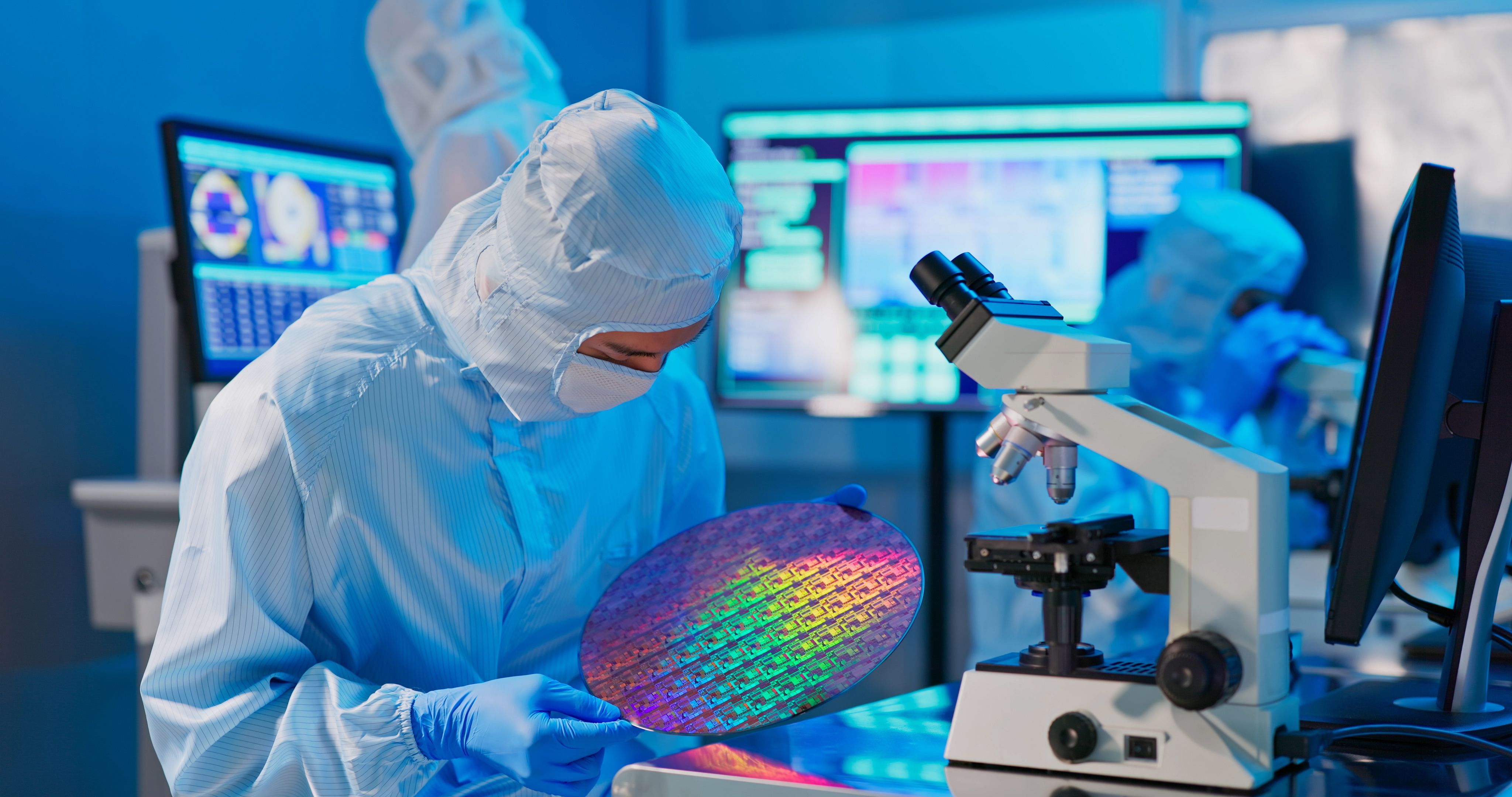
- Semiconductor
- Integrated biology
- Proteomics
- Metabolomics


Major Products/Services
- Cary 630 FTIR
- Mobile and Handheld FTIR
- 610/620 FTIR Microscopy and Imaging
- Cary 8454 UV-Vis Diode Array System
- Cary 60 UV-Vis
- Cary 100/300 UV-Vis
- Cary 4000/5000/6000i UV-Vis-NIR
- Cary 7000 Universal Measurement Spectrophotometer (UMS)
- Cary Eclipse Fluorescence
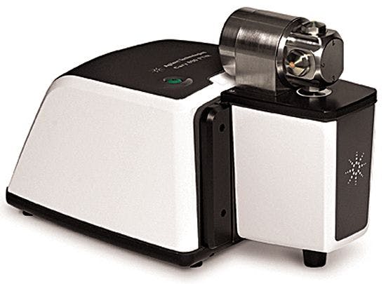
- 490 Micro GC
- 7200 Q-TOF GC–MS
- 200 Series AA systems
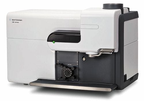
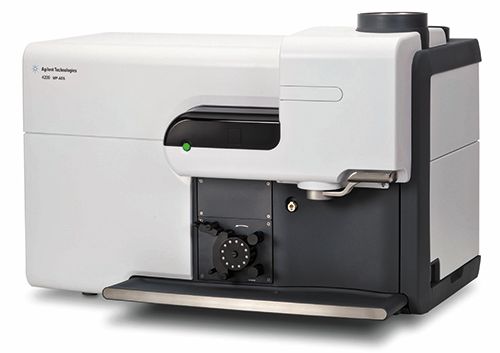
- 4200 MP-AES
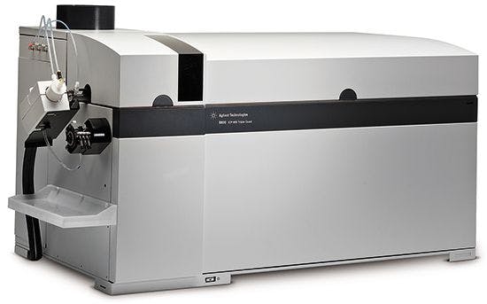
- 5100 ICP-OES
- 7900 ICP-MS
- 7800 ICP-MS
- 8800 ICP-QQQ
- 5977B Series GC-MSD
- 5975T LTM GC-MSD
- 5977E Series GC-MSD
- 6100 Series Single Quad LC–MS
- 6200 Series Accurate Mass TOF LC–MS
- 6400 Series Triple Quad LC–MS
- 6500 Series Accurate Mass Q-TOF LC–MS
- 6560 Ion Mobility Q-TOF LC–MS
- 7000 Series Triple Quadrupole GC–MS
- 7010 Triple Quadrupole GC–MS
- 7200 Q-TOF GC–MS
- MassHunter Software
- EZChrom Elite
- SPS 4 Autosampler
- OneNeb Nebulizer


Facility
Major facilities in Santa Clara, California; Wilmington, Delaware; Melbourne, Australia; Glostrup, Denmark; Waldbronn, Germany; Tokyo, Japan; and Shanghai, China.
Agilent Technologies, Inc.
5301 Stevens Creek Blvd.
Santa Clara, CA 95052
TELEPHONE
(800) 227-9770
(302) 993-5309
FAX
(302) 633-8901
E-MAILcag_sales-na@agilent.com
WEB SITEwww.agilent.com
NUMBER OF EMPLOYEES
12,000
YEAR FOUNDED
1999


Newsletter
Get essential updates on the latest spectroscopy technologies, regulatory standards, and best practices—subscribe today to Spectroscopy.