Using confocal Raman imaging and other advanced measurement techniques, we study the localized strain characteristics of tungsten diselenide (WSe2), an important nanomaterial used for optoelectronic device applications.
Using confocal Raman imaging and other advanced measurement techniques, we study the localized strain characteristics of tungsten diselenide (WSe2), an important nanomaterial used for optoelectronic device applications.

Special Issues
The sensitivity of a high-resolution Raman imaging system is crucial to the quality of the acquired information.
Special Issues
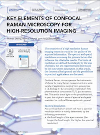
The combination of confocal Raman and atomic force microscopes allows chemical and surface topography imaging of large samples without any ongoing process control by an operator. This article describes the relevant measurement principles and presents examples of automated measurements on nanostructured materials.