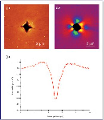
Using confocal Raman imaging and other advanced measurement techniques, we study the localized strain characteristics of tungsten diselenide (WSe2), an important nanomaterial used for optoelectronic device applications.
Using confocal Raman imaging and other advanced measurement techniques, we study the localized strain characteristics of tungsten diselenide (WSe2), an important nanomaterial used for optoelectronic device applications.

Special Issues
Five key qualitative factors–speed, sensitivity, resolution, modularity and upgradeability, and combinability–contribute to the quality of confocal Raman imaging microscopes. Using application examples, this article introduces modern Raman imaging and correlative imaging techniques, and presents state-of-the-art practice examples from polymer research, pharmaceutics, low-dimensional materials research, and life sciences.

Application Notebook
The development of advanced polymeric materials requires detailed information about the phase separation process on the nanometer scale. Confocal Raman microscopy contributes to the analysis of such materials by visualizing the distribution of individual components based on the unique Raman spectra for different polymeric materials. Using a confocal setup, polymer domains can be imaged three-dimensionally with a resolution down to 200 nm. As a Raman image typically consists of tens of thousands of spectra, a powerful data analysis software is essential in order to extract the relevant information. Hidden structures in the images should ideally be visualized automatically, ensuring an objective and consistent interpretation of the imaging data.
Special Issues
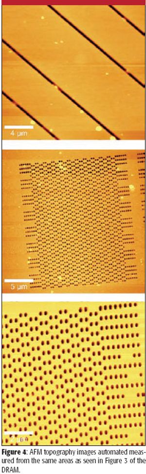
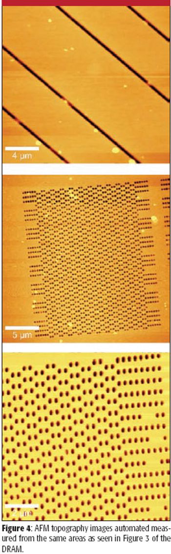
The combination of confocal Raman and atomic force microscopes allows chemical and surface topography imaging of large samples without any ongoing process control by an operator. This article describes the relevant measurement principles and presents examples of automated measurements on nanostructured materials.
Special Issues
Confocal Raman microscopy can be useful when applied to all samples that are heterogeneous on the micrometer to millimeter scale and that generally can be investigated by Raman spectroscopy. This article presents examples of confocal Raman microscopy from various fields of application including pharmaceutical analysis and stress measurements in semiconductors.

September 1st 2009

June 1st 2019