Publication
Article
Spectroscopy
Growth and Temperature-Dependent Spectral Properties of Yb3+, Tm3+ Co-Doped NaY(MoO4)2 Crystal
The NaY(MoO4)2:Yb3+/Tm3+ single crystal was grown by the vertical Bridgman method using spontaneous crystallization. After annealing at 850 °C for 24 h in a muffle furnace under an air atmosphere, the obtained light black crystal became transparent and optically clear. Powder X-ray diffraction (PXRD) confirmed that the as-grown crystal had the structure of scheelite. The segregation coefficients of Tm3+ and Yb3+ were 0.589 and 0.588, respectively. Under 980 nm excitation, the temperature dependence of the emission intensity of the crystal in the temperature range of 298–473 K was measured. The results show that, because of the thermal quenching effect, the emission intensity decreases as the temperature rises. The possible energy transfer modes between Yb3+ and Tm3+ ions were analyzed. The emission cross section was calculated to be 1.97 × 10⁻²⁰ cm2 by the Füchtabauer-Ladeburg formula, and the fluorescence lifetime was fitted to be 166.67 μs.
In recent years, with the rapid development of near-infrared (NIR) optical amplifiers and mid-IR fiber lasers, new rare earth-doped solid IR luminescent materials have attracted great attention (1–5). Among rare earth ions, the energy level transitions of 3H4–3F4 and 3F4–3H6 of Tm3+ can generate fluorescence emission in the bands of 1.47– 1.8 μm (6). The glass fiber with Tm3+ as the luminescence center is a type of material suitable for the third window fiber amplifier, which has a strong energy cross-relaxation effect between Tm3+ ions (3H6, 3H4→3F4,3F4) (7). Tm3+ stimulated radiation belongs to quasi-three-level, and the emission wavelength is in the wavelength range of 1.47–1.8 μm (8–10). However, because of the concentration quenching effect, the symmetric energy level of the Tm3+ ion limits the effective emission of the laser (11,12). The effective way to overcome this shortcoming is to combine with the Yb3+ ion (13–17). Yb3+ is the most promising ion that can be used in all solid-state laser sources in the NIR spectrum around 1030 nm. Compared with other ions, Yb3+ ion is also a good sensitizer, which only has two very simple 2F7/2 and 2F5/2 energy levels and can absorb light near 980 nm (18,19).
In many substrates, such as glass and single crystal, the combination of the Yb3+ ion and the Tm3+ ion is considered to be an effective composition for laser crystals. The doped crystal needs the radius and electronegativity of the cation of the host crystal and the activated ion to be as close as possible. Moreover, a variety of solid-state lasers have been constructed for eye-safe applications using Yb3+ and Tm3+ doped YAG, YLiF4 (20–22). With stable chemical properties, good luminescence properties, high thermal stability, and low phonon energy, sodium yttrium molybdate (NaY[MoO4]2) is considered to be a good luminescent matrix. Considering the above reasons, we studied the Yb3+ and Tm3+ ion co-doped with NaY(MoO4)2. The Yb3+ and Tm3+ ion can replace the Y3+ ion easily, so the Yb3+ and Tm3+ co-doped system could be introduced in the NaY(MoO4)2 crystal (23).
The vertical Bridgman method using spontaneous crystallization is an easily feasible way to obtain crystal samples for measurement (24–26). Here, we used the solid phase synthesis method to synthesize the precursor and the vertical Bridgman method with spontaneous crystallization to grow the NaY(MoO4)2:Re (Re=Yb/Tm) crystal. The thermal annealing, X-ray powder diffraction analysis, absorption spectrum, and temperature dependence emission spectra of the NaY(MoO4)2:Yb3+/Tm3+ crystal is reported in detail in this paper.
Materials and Methods
Materials
The raw materials for crystal growth of NaY(MoO4)2:Yb3+/ Tm3+ were molybdenum oxide (MoO3, 99.99%), sodium carbonate (Na2CO3, 99.99%), ytterbium oxide (Yb2O3, 99.99%), thulium oxide (Tm2O3, 99.99%), and yttrium oxide (Y2O3, 99.99%).
Crystal Growth
The NaY(MoO4)2:Yb3+/Tm3+ precursor for crystal growth was prepared by solid-state reaction according to the following stoichiometric relation:

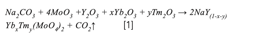

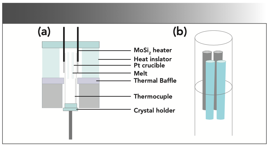
where x and y are the doping concentration. To compensate for the volatilization of MoO3 during solid phase reaction and crystal growth, an additional 0.2at% MoO3 was added. The raw materials were mixed and grounded in a mortar for 2 h. The precursor was put into an alumina crucible and calcined in a muffle furnace at 950 °C for 24 h. The process was repeated, and the samples were held at 1000 °C for 48 h to make an adequate solid-state reaction. The synthesized NaY(MoO4)2:Yb3+/Tm3+ polycrystalline powder was filled into a platinum crucible. The platinum crucible was then placed in a Bridgman growth furnace built in-house for crystal growth. The schematic of the Bridgman growth furnace used in this study was presented in Figure 1a. The obvious advantage of the vertical Bridgman method is that multiple crystals with a smaller size can be grown simultaneously, which helps save time, energy, and raw materials. In this experiment, the position of the four platinum crucibles in the furnace was shown in Figure 1b. The melting point of the NaY(MoO4)2 crystal was 1120 °C (27), and the controlled temperature of the furnace was 1250 °C. The lowering speed of the crucibles was fixed at 0.35 mm/h during the crystal process.

 Schematic of the Bridgman growth furnace, and (b) layout of platinum crucibles in the furnace.")
FIGURE 1: (a) Schematic of the Bridgman growth furnace, and (b) layout of platinum crucibles in the furnace.
Characterization
The structure of the NaY(MoO4)2:Yb3+/Tm3+ crystal was confirmed through powder X-ray diffraction (PXRD), using a diffractometer of Bruker D8 with Cu Kα radiation (λ=1.54056 Å) at room temperature. The measurement was carried out with the scanning step of 0.02°, the scanning scope was from 10° to 80°, the high voltage was 40 kV, and the current was 40 mA. A scanning electron microscope (SEM) with Helios G4 CX model and energy spectrum model called the Edax Apollo X was used to detect the content of the elements in the single crystal. The absorption spectrum in the range of 500–2000 nm was measured by a PerkinElmer UV-visible-NIR (UV-vis-NIR) spectrometer photometer (Lambda-950) with the resolution of 1 nm at room temperature. Under the excitation of 980 nm LD laser, the temperature-dependent emission spectra in the range of 1000–1600 nm were recorded with the Edinburgh FLS920 fluorescence spectrometer, in which the temperature of 273 to 473 K was controlled by Oxford Instruments liquid nitrogen with an isothermal titration calorimetry (ITC) temperature controller and software. The luminescence decay curve was measured by the FL 3–111 fluorescence spectrometer using a gate of 5 μs.
Results and Discussion
Crystal Growth and Powder X-ray Diffraction Analysis
The vertical Bridgman method is a very effective method to obtain the NaY(MoO4)2:Yb3+/Tm3+ crystal. First, the NaY(MoO4)2:Yb3+/Tm3+ crystal crystallized at the bottom of the crucible, so the shape of the crucible affected the spontaneous crystallization of the crystal. The crystal shape obtained by the vertical Bridgman method was similar to that of a crucible. To obtain the single crystal, the bottom of the platinum crucible was squeezed with an angle of approximately 7°, because the spontaneous crystallization could not eliminate the grain boundaries at the large shoulder angle and diameter.
The as-grown crystal showed two colors: light black from the middle to the bottom, and yellow at the top, in which the yellow at the top is polycrystalline, which is shown in Figure 2a. The reason for the yellow color at the top could be the role of transition metals in the raw materials (28). The light black color should be caused by the oxygen vacancies, which were formed by the growth of the crystal in a closed environment (5,29). This process can be explained by the following equation 2:


 NaY(MoO4)2:Yb3+/Tm3+ crystal, and (b) annealed NaY(MoO4)2:Yb3+/Tm3+ crystal sample with the size of 15 × 5 × 1 mm3.")
FIGURE 2: Photographs of (a) NaY(MoO4)2:Yb3+/Tm3+ crystal, and (b) annealed NaY(MoO4)2:Yb3+/Tm3+ crystal sample with the size of 15 × 5 × 1 mm3.
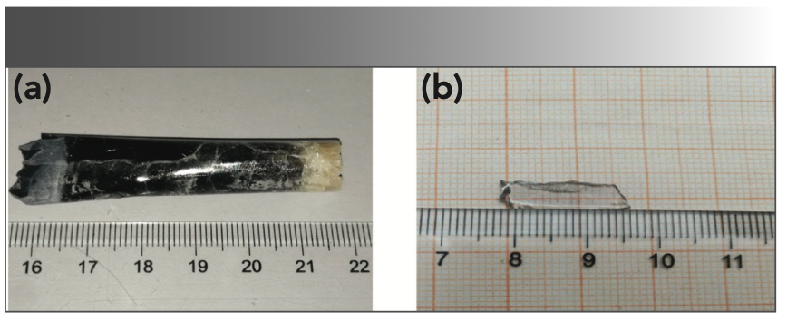
After annealing at 850 °C for 24 h in a muffle furnace under air atmosphere, the obtained light black crystal showed uniform colorlessness and transparency. The reason was that oxygen diffused into the lattice, filling and occupying the oxygen vacancies. The mechanism is shown as the following equation 3:


By cutting and polishing, an optical transparent sheet as shown in Figure 2b was obtained, which was used for testing and analysis.
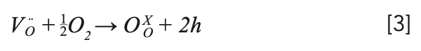
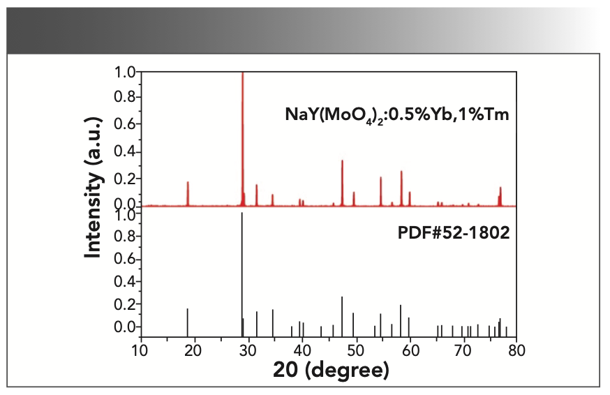
Figure 3 shows the PXRD pattern of NaY(MoO4)2:Yb3+/Tm3+ powder at room temperature with the NaY(MoO4)2 standard card (PDF #82-2369) as a reference. All diffraction peaks match well with the NaY(MoO4)2 standard cards, and no additional diffraction peaks corresponding to any impurities were observed. Figure 4 shows that the crystal belonged to the tetragonal scheelite (CaWO4) structure, and the phase structure of the NaY(MoO4)2 crystal had not changed by doping other rare earth ions. The NaY(MoO4)2:Yb3+/Tm3+ single crystal was a molybdate crystal with scheelite structure, belonging to the tetragonal system, with a I41/a space group and two molecules per unit cell. In this lattice, MoO42- tetrahedral ion groups replaced the positions of the WO42- tetrahedral ion groups. Na+ and Y3+ ions randomly occupied the crystal lattice of Ca2+, and the doping of the Yb3+ and Tm3+ ions did not affect the crystal structure (30–32).

2:Yb3+/Tm3+ crystal.")
FIGURE 3: The PXRD patterns of NaY(MoO4)2:Yb3+/Tm3+ crystal.

2:Yb3+/Tm3+ single crystal.")
FIGURE 4: Schematic cell structure of tetragonal NaY(MoO4)2:Yb3+/Tm3+ single crystal.
Segregation Coefficient
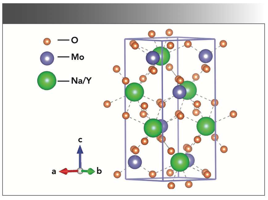
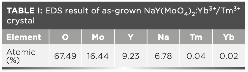
Figure 5 shows the energy-dispersive spectroscopy (EDS) diagram of the as-grown NaY(MoO4)2: Yb3+/Tm3+ crystal, which confirmed that the crystal was mainly composed of six elements: oxygen, molybdenum, yttrium, sodium, thulium, and ytterbium. Table I shows the atomic percent of the above six elements.

2:Yb3+/Tm3+ crystal.")
FIGURE 5: EDS analysis of as-grown NaY(MoO4)2:Yb3+/Tm3+ crystal.


The segregation coefficients K of Tm3+ and Yb3+ in NaY(MoO4)2: Yb3+/Tm3+ crystal were calculated by equation 4:

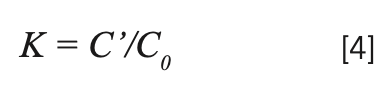

C' and C0 are the concentrations of rare earth ions in the crystal and raw material, respectively. Table II shows the results of NaY(MoO4)2:Yb3+/Tm3+. The separation coefficient represents the extent to which the dopant occupies the host ion lattice, which depends on the difference of the charge, radius, and properties between the doped and host ions. The closer the separation coefficient is to 1, the more uniform the concentration within the grown crystal.


In this paper, the segregation coefficients of Tm3+ and Yb3+ ions in NaY(MoO4)2:Yb3+/Tm3+ single crystal are 0.589 and 0.588, respectively, indicating that the concentrations of dopants in different parts during the crystal growth are not uniform. It is reasonable to calculate the spectral parameters using the average concentration of doped ions.
Absorption Spectra of NaY(MoO4)2 Crystal Co-Doped by Yb3+ and Tm3+ Ions
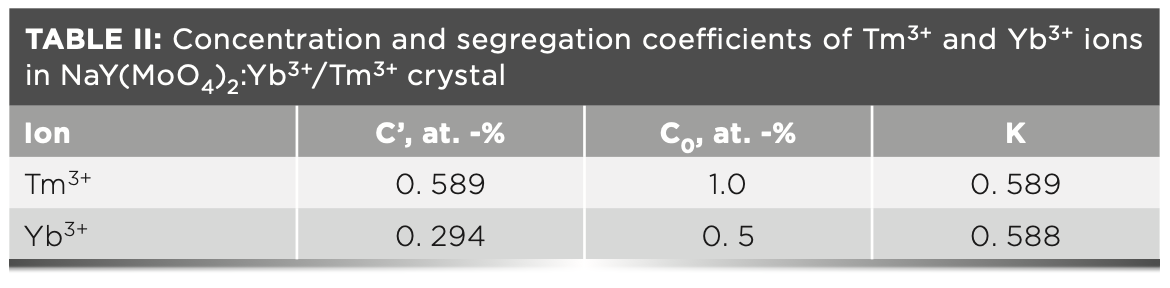
Figure 6 shows the absorption spectrum of the annealed NaY(MoO4)2: Yb3+/Tm3+ crystal sample at room temperature. The spectrum ranging from 500 to 2000 nm consisted of the absorption bands near 692, 798, 1220, and 1753 nm, which were corresponding to the transitions from the ground state 3H6 to the excited states 2F2/3, 3H4, 3H5, and 3F4 of Tm3+, and near 866 nm was corresponding to the transitions from the ground state 2F7/2 to the excited state 2F5/2 of Yb3+.

2 crystal co-doped by Yb3+ and Tm3+ ions.")
FIGURE 6: The absorption spectrum of NaY(MoO4)2 crystal co-doped by Yb3+ and Tm3+ ions.
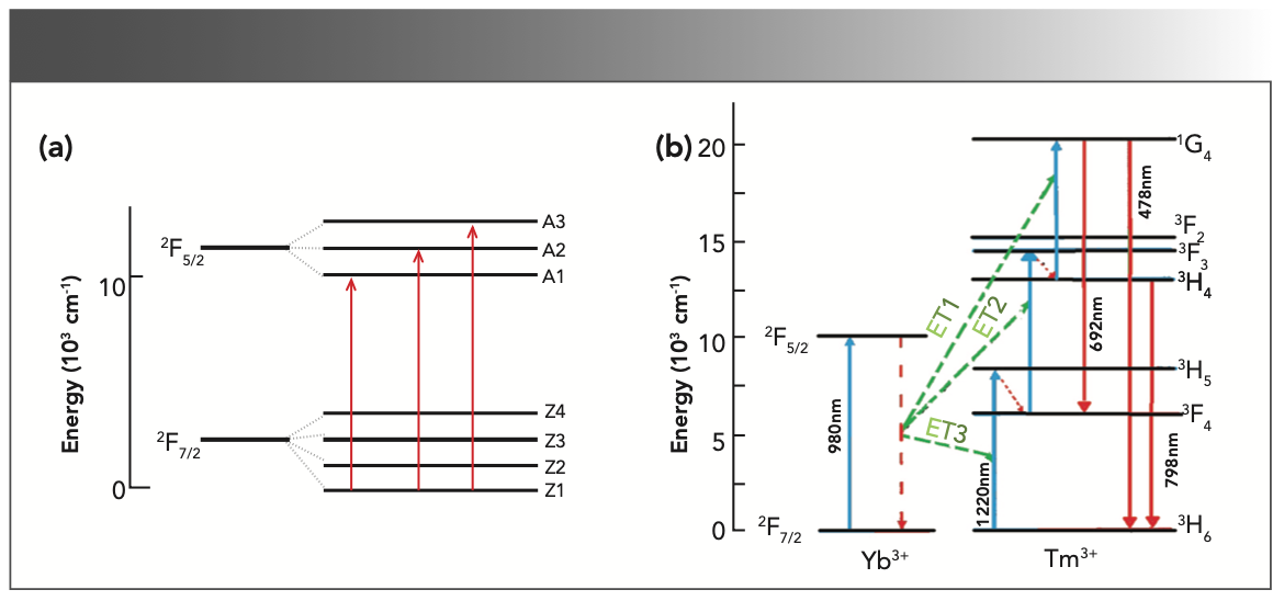
It can be seen from Figure 6 that the absorption of Yb3+ ions forms an absorption band between 856 and 1022 nm, which is because in the NaY(MoO4)2 crystal, the Stark splitting of the crystal field, 2F5/2 and 2F7/2 of Yb3+, form the upper and lower two-state clusters, namely the upper-state cluster 2F5/2 and the lower-state cluster 2F7/2, in which the energy level difference is approximately 10,000 cm-1.
The absorption cross section of rare earth ions is very important for analyzing the performance of solid-state lasers and amplifiers doped with rare earth ions. We can calculate the absorption cross section by the measured optical absorption OD(λ) (7):

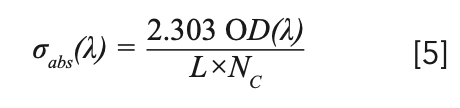

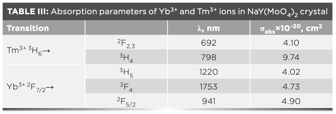
where σabs(λ) is the absorption cross-section, OD(λ) is the optical density, L is the thickness of sample and Nc is the density of Tm3+ (2.83 × 1021 cm-3) or Yb3+ (1.43 × 1021 cm-3). The wavelengths of the observed absorption peaks and the corresponding absorption cross-sections are listed in Table III.


Temperature-Dependent Emission Spectra and Cross-Section
The thermal emission stability of the crystal is an important aspect in the NIR laser field. To investigate the temperature-dependent emission spectra of the NaY(MoO4)2:Yb3+/Tm3+ crystal at different temperatures, the annealed NaY(MoO4)2:Yb3+/Tm3+ crystal was excited by a 980 nm LD laser in the range of 298–473 K. The emission intensity of the crystal gradually increased from 473 to 373 K, and sharply increased from 373 K to room temperature, which could be observed from 1000 to 1600 nm in Figure 7.

2:Yb3+/Tm3+ crystal.")
FIGURE 7: Temperature-dependent emission spectra of the annealed NaY(MoO4)2:Yb3+/Tm3+ crystal.
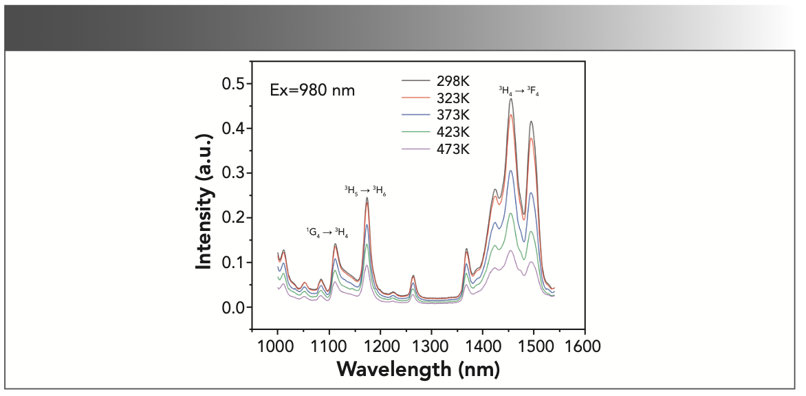
Under the 980 nm excitation, NaY(MoO4)2:Yb3+/Tm3+ contains three additional emission bands near 1112, 1174, and 1455 nm, which are corresponding to 1G4(Tm3+)→3H4(Tm3+) transition, 3H5(Tm3+)→3H6(Tm3+), and 3H4(Tm3+)→3F4(Tm3+), respectively. As shown from Figure 7, the emission peak intensity at 1455 nm is close to that at 1495 nm, and the intense emission peaks are centered at 1455 nm.
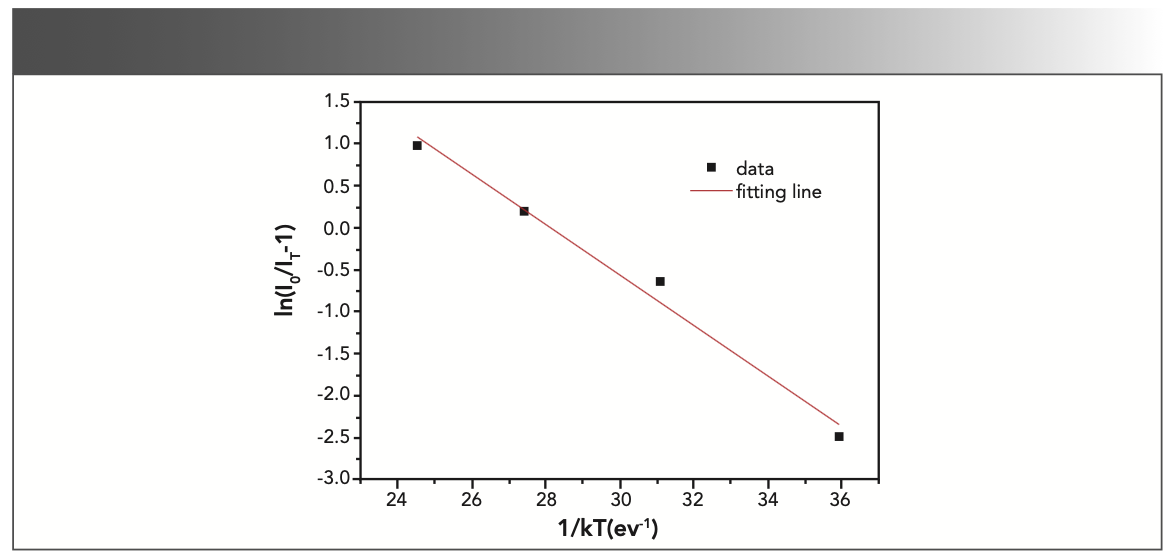
To explain the temperature dependent photoluminescence, activation energy was calculated through the Arrhenius equation 6 (33):

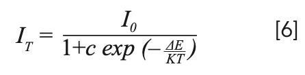

where I0 is the emission intensity at room temperature; IT is the emission intensity at measurement temperature; c is a constant; K is the Boltzmann constant (8.617 × 10⁻⁵ eV/K); and ΔE is the activation energy for thermal quenching. The fitting line of In[I0/IT-1] versus 1/kT is illustrated in Figure 8. The ΔE of NaY(MoO4)2 co-doped by Yb3+ and Tm3+ ions was calculated to be 0.301 eV. Compared to our previous work, where the ΔE of NaY(MoO4)2:Er3+ co-doped by Tm3+ was calculated to be 0.234 eV (10), the thermal emission NaY(MoO4)2:Yb3+/Tm3+ crystal increased.

![FIGURE 8: A ln[I0/IT) − 1] vs. 1/kT activation energy graph for the thermal quenching of NaY(MoO4)2:Yb3+/Tm3+ crystal.](/_next/image?url=https%3A%2F%2Fcdn.sanity.io%2Fimages%2F0vv8moc6%2Fspectroscopy%2F8e1e4d18f19caebaedfc6ef7da5802b0463e9385-1174x560.png%3Ffit%3Dcrop%26auto%3Dformat&w=3840&q=75 "FIGURE 8: A ln[I0/IT) − 1] vs. 1/kT activation energy graph for the thermal quenching of NaY(MoO4)2:Yb3+/Tm3+ crystal.")
FIGURE 8: A ln[I0/IT) − 1] vs. 1/kT activation energy graph for the thermal quenching of NaY(MoO4)2:Yb3+/Tm3+ crystal.
When the temperature rose, the carriers, which were fixed in the traps, were released to the emitting center (Yb3+, Tm3+). Therefore, the electron-phonon interaction was the main one, exciting Yb3+, and the Tm3+ luminescence center was activated by the interaction of the phonon, which was obtained by the cross release between the excited state and the ground state. Therefore, as the temperature rose, the emission intensity of the crystal decreased. Therefore, the crystal exhibited a non-radiative transition (27). The emission cross section is an important parameter for evaluating the possibility of laser action. A larger emission cross section means a higher light output. The emission cross section σem was calculated by the Füchtabauer-Ladeburg (F-L) formula (34):


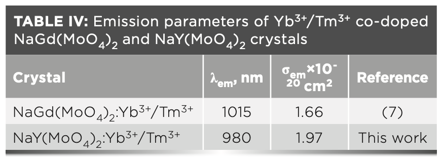
where τ is the decay time; n is the refractive index, which can be calculated by the following formula: n2 = 3.8770 + 62950/(λ2 - 42981) (35); λ is the wavelength; I(λ) is the relative fluorescence intensities as a function of wavelength; and c is the velocity of light. The peak value of fluorescence cross-sections calculated by equation 7 is 1.97 × 10⁻²⁰ cm2 for NaY(MoO4)2:Yb3+/Tm3+ crystal at 1455 nm. The emission cross-section of Yb3+ and Tm3+ co-doped NaY(MoO4)2 calculated from equation 7, which is compared with the NaGd(MoO4)2 crystal, is listed in Table IV.


The electronic configuration is [Xe]4f12, and its ground state spectrum item is 3H4. Furthermore, its spectrum items were 3H, 3F, and 1G; through spin-orbit coupling, each spectrum branch item was formed. Under the excitation of 980 nm, the NaY(MoO4)2:Yb3+/Tm3+ crystal has a strong emission band at 1453 nm, which corresponded to the transition from 3H4 (Tm3+) to 3F4 (Tm3+). It can be seen from Figure 8 that the intensity of the emission peak at 1453 nm was close to the intensity of the emission peak at 1496 nm, so 1453 and 1493 nm in the NaY(MoO4)2:Yb3+/Tm3+ crystal can better overlap to form ultra-wide NIR luminescence.
Energy Transfer and Fluorescence Decay Curves
Tm3+ ions formed an absorption band between 1187~1216 nm and 1701~1800 nm under the pump of 980 nm LD. First, the Yb3+ ion absorbed a photon through ground state absorption (GSA) to generate the 2F7/2→2F5/2 transition, and then the excited Yb3+ ion transferred its energy to the 2F5/2 energy level. Through mass transfer (ET) to Tm3+, the ground state 3H6 level was excited to the 3H5 level through ground state absorption (GSA). The 3H5 and 3F4 energy levels were similar (the difference is approximately 2000 cm-1). Because the difference between the 3F2 and 3F4 energy levels of Tm3+ is similar to the 2F5/2 energy of Yb3+, the excited state Tm3+ at the 3F4 energy level transitions to the 3F2 energy level through excited state absorption (ESA), and 3F2/3 then relaxes through multi-phonon relaxation (MR) and returns to the 3H4 level. At the 3H4 excited state energy level, Tm3+ can continue to transition to 1G4 energy level through ESA, or it can return to the ground state 3H6 and emit a photon with a wavelength of approximately 795 nm. Tm3+ in the excited state 1G4 produces a 692 nm up-conversion red light rare earth ion up-conversion luminescence through a radiation transition to 3F4. Figure 8b shows the energy level diagram and possible up-conversion transition process of the Yb3+ and Tm3+ co-doped sample under 980 nm excitation. According to the energy matching mechanism, the transitions that produce red light 1G4→3F4 and NIR light 3H4→3H6 can be explained as follows:

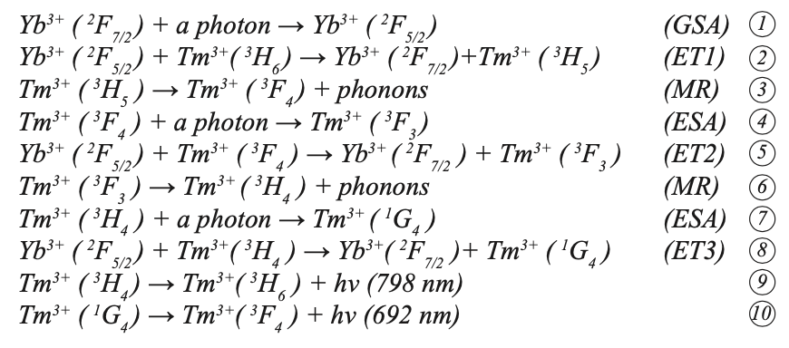

where h is the Planck constant and ʋ is the frequency. Because the energy difference between the transition between Yb3+:2F5/2→2F7/2 and Tm3+: 3H6→3H5, 3F4→3F2, 3H4→1G4 does not match, the ET between Yb3+ and Tm3+ is a rope assist energy transfer. It can be seen from the above that the up-conversion near-infrared light (3H4→3H6 transition) is a two-photon absorption process. Up-converting blue light (1G4→3H6 transition) and red light (1G4→3F4 transition) are three-photon absorption processes, and up-converting blue light is not reflected in the figure. In addition, the energy levels of 3H5 and 3F2, 3 are very short-lived. The ions in these energy levels can quickly and non-radiatively transit to the 3F4 and 3H4 energy levels, making reverse energy difficult to perform because of the processes 2, 4, and 8. The process has high energy transfer efficiency. Therefore, the Yb3+ and Tm3+ co-doped NaY(MoO4)2 crystal can produce strong near infrared light emission (798 nm) under the excitation of 980 nm LD pump, which is consistent with the transition mechanism in Figure 9.

 Stark level splitting of Yb3+ energy level diagram, and (b) possible up-conversion luminescence mechanism of Yb3+ and Tm3+ co-doped NaY(MoO4)2 crystal.")
FIGURE 9: (a) Stark level splitting of Yb3+ energy level diagram, and (b) possible up-conversion luminescence mechanism of Yb3+ and Tm3+ co-doped NaY(MoO4)2 crystal.
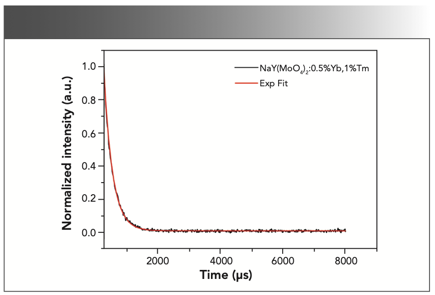
The fluorescence attenuation curve of the NaY(MoO4)2:Yb3+/Tm3+ crystal after annealing was measured as shown in Figure 10. The curve of the crystal can be calculated by fitting an exponential function:


where I0 is the initial spectral intensity and τ is the decay time constant of the emission. Hence, the decay time from the emission line 3H4→3F4 at 1455 nm of the NaY(MoO4)2:Yb3+/Tm3+ crystal after annealing is fitted to be 166.67 μs. The fluorescence lifetime of co-doped sample was shorter, which was mainly because of the energy transition between ions in a shorter time.

2:Yb3+/Tm3+ fitted using exponential functions at room temperature.")
FIGURE 10: The fluorescence decay curves of NaY(MoO4)2:Yb3+/Tm3+ fitted using exponential functions at room temperature.
Conclusion
The NaY(MoO4)2 crystal co-doped by Yb3+ and Tm3+ ions have been grown by the vertical Bridgman method using spontaneous crystallization. The grown doped NaY(MoO4)2 crystal appeared dark brown in color, and the PXRD pattern confirms that the crystal structure was tetragonally symmetric with I41/a space group. The NaY(MoO4)2 co-doped crystal enriches the emission band in the near-infrared region, and improves the pump energy absorption efficiency at 980 nm. In addition, as the temperature dropped from 473 K to room temperature under 980 nm LD laser excitation, the emission intensity increased. Therefore, NaY(MoO4)2:Yb3+/Tm3+ crystal as a NIR laser crystal has a strong potential application prospect in optics and photonic devices.
Acknowledgments
This work was sponsored by National Natural Science foundation of China (No. 61875096 and 61775108).
References
(1) L. Dai, Y. Shao, C. Liu, R. Chen, X. Han, and S. Yang, Opt. Mater. 95, 109193 (2019).
(2) J. Pisarska, R. Lisiecki, W. Ryba-Romanowski, G. Dominiak-Dzik, and W.A. Pisarski, J. Alloys Compd. 451, 226–228 (2008).
(3) R. Soulard, J.L. Doualan, A. Braud, M. Sahli, A. Benayad, G. Brasse, A. Hideur, A. Tyazhev, R. Moncorgé, and P. Camy, Opt. Mater. 72, 578–582 (2017).
(4) G. Jiang, X. Wei, Y. Chen, C. Duan, and M. Yin, J. Rare Earths 31, 27–31 (2013).
(5) R.A. Talewar, V.M. Gaikwad, P.K. Tawalare, and S.V. Moharil, Opt. Laser Technol. 115, 215–221 (2019).
(6) Z.J. Wang, X.Z. Li, G.J. Wang, M.J. Song, Q. Wei, G.F. Wang, and X.F. Long, J. Lumines. 128, 451–456 (2008).
(7) Z.J. Wang, X.Z. Li, Q. Wei, and X.F. Long, Mater. Res. Innovations 12, 174–178 (2013).
(8) Y. Ohishi, A. Mori, M. Yamada, H. Ono, Y. Nishida, and K. Oikawa, Opt. Lett. 23, 274–276 (1998).
(9) P. Peterka, B. Faure, W. Blanc, M. Karásek, and B. Dussardier, Opt. Quantum Electron. 36, 201–212 (2004).
(10) Z. Chen, J. Zhang, S. Pan, X. Wang, and J. Pan, J. Lumines. 225, 117347 (2020).
(11) M.P. Hehlen, A. Kuditcher, A.L. Lenef, H. Ni, Q. Shu, S.C. Rand, J. Rai, and S. Rai, Phys. Rev. B 61, 1116–1128 (2000).
(12) S.D. Jackson and S. Mossman, Appl. Opt. 42, 2702–2707 (2003).
(13) A. Braud, S. Girard, J.L. Doualan, M. Thuau, R. Moncorgé, and A.M. Tkachuk, Phys. Rev. B 61, 5280–5292 (2000).
(14) L. Feng, Q. Tang, L. Liang, J. Wang, H. Liang, and Q. Su, J. Alloys Compd. 436, 272–277 (2007).
(15) M. Liao, L. Wen, H. Zhao, Y. Fang, H. Sun, and L. Hu, Mater. Lett. 61, 470–472 (2007).
(16) X. Mateos, R. Solé, J. Gavaldà, M. Aguiló, J. Massons, and F. Díaz, Opt. Mater. 28, 423–431 (2006).
(17) W. Xu, X. Xu, W. Feng, G. Zhao, Z. Zhao, G. Zhou,and J. Xu, Opt. Commun. 272, 182–185 (2007).
(18) H. Cañibano, G. Boulon, L. Palatella, Y. Guyot, A. Brenier, M. Voda, R. Balda, and J. Fernandez, J. Lumines. 102-103, 318–326 (2003).
(19) Y.K. Voron’Ko, K.A. Subbotin, V.E. Shukshin, D.A. Lis, S.N. Ushakov, A.V. Popov, and E.V. Zharikov, Opt. Mater. 29, 246–252 (2006).
(20) C. Borel, Opt. Commun. 142, 239–243 (1997).
(21) W.A. Bollig, R.A. Clarkson, and D.C. Hayward, Opt. Commun. 154, 35–38 (1998).
(22) P. Song, Z. Zhao,X. Xu, B. Jang, P. Deng, and J. Xu, J. Cryst. Growth 270, 433–437 (2004).
(23) N.Y. Garces, M.M. Chirila, H.J. Murphy, J.W. Foise, E.A. Thomas, C. Wicks, K. Grencewicz, L.E. Halliburton, and N.C. Giles, J. Phys. Chem. Solids 64, 1195–1200 (2003).
(24) D.J. Daniel, H.J. Kim, S. Kim, and S. Khan, Opt. Mater. 70, 120–126 (2017).
(25) Y. Dong, H. Xia, L. Fu, S. Li, X. Gu, J. Zhang, D. Wang, Y. Zhang, H. Jiang, and B. Chen, Optoelectron. Lett. 10, 262–265 (2014).
(26) P. Yu, L. Su, H. Zhao, X. Guo, H. Li, X. Feng, Q. Yang, and J. Xu, Opt. Mater. 33, 831–834 (2011).
(27) J. Zhang, I.R. Pandey, S. Pan, H. Kim, J. Pan, and H. Chen, J. Lumines. 212, 184–190 (2019).
(28) S. Pan, J. Zhang, J. Pan, G. Ren, J. Lee, and H. Kim, J. Cryst. Growth 498, 56–61 (2018).
(29) X. Wang, Z. Li, K. Li, L. Zhang, J. Cheng, and L. Hu, Opt. Mater. 35, 2290–2295 (2013).
(30) A. Méndez-Blas, M. Rico, V. Volkov, C. Cascales, C. Zaldo, C. Coya, A. Kling, and L.C. Alves, J. Phys. Condens. Matter 16, 2139–2160 (2004).
(31) C. Cascales, M. Serrano, F. Estebanbetegón, C. Zaldo, R. Peters, K. Petermann, G. Huber, L. Ackermann, D. Rytz, and C. Dupré, Phys. Rev. B 74, 3840–3845 (2006).
(32) M. Rico, U. Griebner, V. Petrov, P. Ortega, X.M. Han, C. Cascales, and C. Zaldo, J. Opt. Soc. Am. B 23, 1083–1090 (2006).
(33) P. Shi, Z. Xia, M.S. Molokeev, and V.V. Atuchin, Dalton Trans. 43, 9669–9676 (2014).
(34) J. Huang, J. Huang, Y. Lin, X. Gong, Y. Chen, Z. Luo, and Y. Huang, J. Lumines. 187, 235–239 (2017).
(35) X. Li, Z. Lin, L. Zhang, and G. Wang, Opt. Mater. 29, 728–731 (2007).
Xi Wang, Zongyue Chen, Jianyu Zhang, and Shangke Pan are with the State Key Laboratory Base of Novel Function Materials and Preparation Science at the School of Material Sciences and Chemical Engineering of Ningbo University, in Ningbo, Zhejiang, China. Shangke Pan and Jianguo Pan are with the Key Laboratory of Photoelectric Materials and Devices of Zhejiang Province, in Zhejiang, China. Direct correspondence to: panshangke@nbu.edu.cn ●


 Bonds")


Newsletter
Get essential updates on the latest spectroscopy technologies, regulatory standards, and best practices—subscribe today to Spectroscopy.


![Figure 3: Plots of lg[(F0-F)/F] vs. lg[Q] of ZNF191(243-368) by DNA.](https://cdn.sanity.io/images/0vv8moc6/spectroscopy/a1aa032a5c8b165ac1a84e997ece7c4311d5322d-620x432.png?fit=crop&auto=format)

