
|Articles|February 1, 2020
- Application Notebook-02-02-2020
- Volume 35
- Issue 2
Gallium Nitride Quality and Stress Field Characterization with 3D Confocal Raman Imaging
Author(s)WITec GmbH
Experimental Conditions
A GaN sample grown on a sapphire substrate featuring hexagonal pits, courtesy of Dr. Eberhard Richter (Materials Technology Department of the Ferdinand Braun Institute, Berlin, Germany), was investigated, and stress fields were visualized. All measurements were carried out using a WITec alpha300 R confocal Raman microscope with an excitation wavelength of 532 nm and a UHTS 300 spectrometer.
Results and Conclusion
A 2D depth scan was performed and the resulting Raman image (Figure 1A) was color coded according to the measured spectra (Figure 1B). The red spectrum shows features typical of GaN and is dominant at the sample surface, showing that the crystal grown there was high in quality. The green spectrum shows enhanced fluorescence at low wavenumbers and is found only at the substrate pit walls. The blue spectrum measured above the pits is distinct from the red one (Figure 1B, inset). The A1(LO) peak is upshifted and broadened compared to the red spectrum, indicating a lower quality GaN crystal.
Next, a stack of 2D scans was performed at different focal planes. Figure 1C shows one layer from the stack. A 3D representation was generated from the image stack (Figure 1D). The fluorescence signal (green) forms rings at the walls of the pits, while the tops of the pits are dominated by the distorted GaN spectrum (blue). The topmost layers show an undistorted GaN spectrum (red).
In order to reveal stress fields in the GaN sample, a peak shift analysis was performed for the entire z-stack. The position of the E2high peak near 570 cm-1 was quantified for each spectrum by fitting a Lorentzian function. Figure 2 shows the same sample volume as in Figure 1D, but color coded according to the determined peak position. The stress fields propagate from the interface to the surface mainly in tube-like structures, which become narrower towards the surface, again indicating higher crystal quality. However, the overall differences in the peak positions were quite small (<1 cm-1) and thus, the overall differences in the strain of the GaN crystal were also small. Nevertheless, the peak shift sensitivity was sufficient to measure and visualize them.
WITec GmbH
Lise-Meitner-Str. 6, D-89081 Ulm, Germany
tel. +49 (0) 731 140 700; +49 (0) 731 140 70 200
Website:
Articles in this issue
over 6 years ago
Vol 35 No 2 Spectroscopy Feb 2020 Application Notebook PDFover 6 years ago
A Robust, High Performance, Revolutionary Demountable ICP Torchover 6 years ago
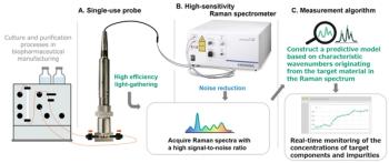
Bioreactor Fermentation Monitoring with Raman SpectroscopyRelated Content


Trending on Spectroscopy Online
1
Evaluating Surface-Enhanced Raman Spectroscopy as a Potential Blood-Based Tool for Crohn’s Disease Detection
2
Microplastics Found in All Commercial Salt Samples Tested in South Sumatra Study
3
Pathways in Spectroscopy: Connecting Students to Valuable Internships
4
Machine Learning Tool Detects Invisible Wood Coating Decay Before Visible Damage Appears
5