EDAX Inc
Company Description
EDAX is a leading provider of innovative materials characterization systems encompassing energy dispersive spectrometry (EDS), wavelength dispersive spectrometry (WDS), electron backscatter diffraction (EBSD), and X-ray fluorescence (XRF). EDAX products include standalone tools for EDS, EBSD and WDS, and integrated tools for EDS/EBSD, EDS/WDS, and EDS/EBSD/WDS. The company offers several XRF and micro-XRF elemental analyzers for small and microspot X-ray analysis and mapping. The XLNCE X-ray metrology line provides in-line instrumentation for process control and yield management for coating applications. EDAX develops the best solutions for micro- and nano-characterization, where elemental and/or structural information is required, making analysis easier and more accurate. EDAX designs, manufactures, distributes, and services products for a broad range of industries, educational institutions, and research organizations.

Chief Spectroscopic Techniques Supported
- Energy dispersive spectroscopy (EDS)
- Energy dispersive X-ray fluorescence (XRF)
- Electron backscatter diffraction (EBSD)
- Wavelength dispersive spectroscopy (WDS)
Markets Served
EDAX instrumentation for elemental and structural analysis is found in a broad spectrum of industrial, academic, and government applications from the field or production line to the most advanced research and development laboratory. Typical markets served include semiconductor and microelectronics, academic and industrial R&D laboratories, RoHS/WEEE renewable energy, pharmaceuticals, mining, security, forensics, catalysts, petrochemicals, metallurgy, and manufacturing operations.
Major Products/Services
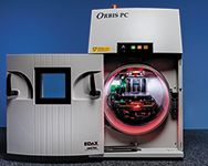
Energy dispersive X-ray fluorescence: EDAX manufactures XRF analyzers both for the laboratory and for coating analysis in industry.
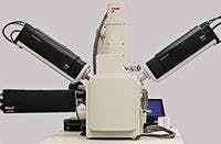
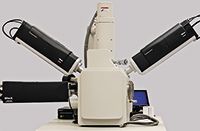
Electron backscatter diffraction: EDAX supplies instrumentation for materials structural analysis on scanning electron microscopes (SEM).
Energy dispersive spectroscopy: EDAX provides a full range of EDS products for elemental analysis on SEMs.
Wavelength dispersive spectroscopy: EDAX offers parallel beam WDS products for elemental analysis on SEMs.


Facility
EDAX headquarters is located in Mahwah, New Jersey, housing sales, engineering, technical support, and operations. EDAX is committed to providing the best possible support for our customers world-wide with sales, service, and applications support offices located in Japan, China, Singapore, The Netherlands, Germany, the United Kingdom, and the United States.


EDAX Inc.
91 McKee Drive
Mahwah, NJ 07430
TELEPHONE
(201) 529-4880
FAX
(201) 529-3156
WEB SITE
YEAR FOUNDED
1962


Newsletter
Get essential updates on the latest spectroscopy technologies, regulatory standards, and best practices—subscribe today to Spectroscopy.


Scientists Use Water and Light to Uncover Honey Adulteration
July 30th 2025In a 2025 study, Indian researchers demonstrated that combining near-infrared (NIR) spectroscopy with aquaphotomics enables rapid, non-destructive detection of adulterants in honey by analyzing changes in water’s spectral behavior. Using chemometric models, they accurately identified and quantified six common adulterants, offering a powerful tool for food authenticity and quality control.


Scientists Use AI and Spectroscopy to Detect Fake Honey in Bangladesh
July 29th 2025Researchers in Bangladesh have developed a rapid, non-destructive method to detect honey adulteration using UV-Vis-NIR spectroscopy paired with machine learning. Their findings could protect consumers and support food quality enforcement.


