Article
Spectroscopy
Spectroscopy
Photoluminescence Spectroscopy Using a Raman Spectrometer
Author(s):
Photoluminescence can provide information about the composition and solid state structure of a material. The high spectral resolution of a Raman spectrometer can be useful in performing photoluminescence spectroscopy of solid state materials, particularly when the emission spectra consist of narrow bands or even lines. Having the capability to perform photoluminescence and Raman spectroscopies simultaneously with the same instrument is advantageous, especially when studying 2D crystals. When used to perform photoluminescence spectroscopy, the Raman spectrometer becomes two instruments in one.
Photoluminescence can provide information about the composition and solid-state structure of a material. The high spectral resolution of a Raman spectrometer can be useful in performing photoluminescence spectroscopy of solid-state materials, particularly when the emission spectra consist of narrow bands or even lines. Having the capability to perform photoluminescence and Raman spectroscopies simultaneously with the same instrument is advantageous, especially when studying two-dimensional (2D) crystals. When used to perform photoluminescence spectroscopy, the Raman spectrometer becomes two instruments in one.
Raman scattering is a weak phenomenon and that is sometimes the reason for being unable to acquire a Raman spectrum, particularly at a low concentration or with a limited amount of sample. However, the most frequent reason for not being able to acquire a Raman spectrum is because a strong fluorescent background and the detector noise generated by it overwhelms the Raman signal. Therefore, it should be self-evident that a Raman spectrometer is ideal for performing laser-excited photoluminescence. In a recent installment of “Molecular Spectroscopy Workbench,” we examined the choice of excitation wavelength to avoid photoluminescence (1). Here we discuss the use of a Raman spectrometer with the express purpose of performing photoluminescence spectroscopy.
The light illuminating a sample must be in resonance with an electronic transition of the material for photoluminescence to occur. More specifically, the sample must absorb a photon of the incoming light to promote an electron from the ground electronic state in a molecule or valence band in a solid to the first excited molecular electronic state or conduction band in a solid, respectively. After the electron is in the excited electronic state or conduction band, it can undergo either radiationless decay or a photon can be emitted as the electron returns to the ground state or valence band. The latter emission process is called photoluminescence because the excited state was reached through the absorption of a photon. In contrast, had the electron been promoted from the valence to the conduction band through the application of a voltage and the passage of current, the subsequent emission would be more properly described as electroluminescence. Photoluminescence occurs in many bulk materials that are direct band gap semiconductors and also because of impurities that absorb and emit light in an otherwise transparent medium. We discuss examples of both situations in this installment.
Chromium Impurities in Aluminum Oxide
The aluminum oxide alumina (Al2O3) is known as corundum in its single crystal form. Within corundum the Al-O bond is approximately 60% ionic and 40% covalent with an Al atom at the center surrounded by six O atoms to form a distorted octahedron (2). Therefore, the aluminum atoms in the crystal can be assigned a formal oxidation state of +3 with the surrounding O atoms each with a -2 formal oxidation state. Pure corundum is colorless; however, Al2O3 is often tinted or even deeply colored because of transition metal impurities in the crystal. Their presence at even less than 1% in the Al2O3 host lattice leads to the beautiful colors seen in gemstones such as ruby and sapphire. The presence of Cr3+ in Al2O3 is what gives ruby its red color, whereas sapphire, also a host crystal of corundum Al2O3, obtains its color from titanium impurities. The electron configuration of the Cr atom is [Ar] 3d5 4s1. When occupying an Al site in the corundum crystal lattice, however, the electron configuration of Cr3+ is [Ar] 3d3 thereby allowing t2g-eg absorption and emission electronic transitions in the 3d orbitals. These electronic transitions are affected by the crystal field of the host lattice, which are then manifest in the absorption and emission spectra.
The combination of Raman and photoluminescence spectroscopies allows one to characterize the host crystal and the transition metal impurities, respectively. Raman spectra acquired from the same location of an Al2O3 crystal using 532-nm and 633-nm excitation are shown in Figure 1. Both spectra consist of Raman bands from the Al2O3 crystal at 144, 417, 568, and 734 cm-1. However, the spectrum excited with 532-nm light has no background whereas that excited at 633 nm manifests a steadily increasing background beginning at approximately 150 cm-1. Furthermore, distinct broad peaks (relative to the Raman bands) appear at approximately 640 and 870 cm-1. The appearance of these two broad peaks in the 633-nm-excited spectrum and their absence in the 532-nm-excited spectrum is confirmation that they are due to photoluminescence and not Raman scattering. The use of different excitation wavelengths with the same sample is one of the best ways to differentiate photoluminescence from Raman scattering. Raman bands appear at the same position, independent of the excitation wavelength, when plotted on a Raman shift scale. However, if the bands appear at different Raman shifts, they are likely caused by photoluminescence. Now plot these same spectra on an absolute wavelength scale. If the bands appear at the same position when plotted on an absolute wavelength scale, their assignment as photoluminescent bands is confirmed.

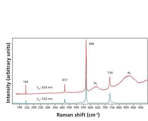
Figure 1: Raman spectra acquired from the same location of single-crystal Al2O3 using excitation wavelengths of 532 nm (green spectrum) and 633 nm (red spectrum). The bands marked PL are caused by photoluminescence.
The peaks at 640 and 870 cm-1 (659.5 and 669.7 nm, respectively) of the Raman spectrum are not the only or even primary emissions from this crystal of Al2O3. The photoluminescence spectra shown in Figure 2 were acquired using 405-, 532-, and 633-nm excitation. All of the spectra shown in this and other figures were acquired using a Horiba LabRAM HR Evolution spectrometer with an 800-mm focal length and 1800-gr/mm gratings. Peaks appear at 692.8 nm and 694.2 nm for all excitation wavelengths when plotted on an absolute wavelength scale. The peak at 810 nm in the spectrum excited at 405 nm is from the grating’s second-order diffraction of the 405-nm laser light. The inset plot with expanded scale of the spectrum excited at 532 nm shows how well resolved the peaks are even though they are separated by only 1.4 nm. The high spectral resolution of a Raman spectrometer allows one to resolve these narrow and closely spaced emissions. This particular pair of strong emissions is quite familiar and arises from Cr3+ impurities commonly found in Al2O3. In fact, if you take almost any piece of Al2O3 optical flat or window and illuminate it with visible laser light, you are likely to observe these same two emissions, confirming that it is actually Al2O3:Cr3+.

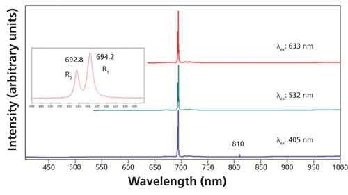

Figure 2: Photoluminescence spectra acquired from the same location of single-crystal Al2O3 using excitation wavelengths of 405 nm (blue spectrum), 532 nm (green spectrum), and 633 nm (red spectrum).
Without sufficient spectral resolution, the emission from Al2O3:Cr3+ can sometimes appear as a single line, known as the R line fluorescence of ruby, in a transition from the excited 2E energy level to the 4A2 level. However, the 2E level can undergo fine splitting because of distortions of the octahedral symmetry thereby producing two closely spaced emissions. These two Al2O3:Cr3+ peaks are well known as R1 (1.788 eV, 693.5 nm) and R2 (1.791 eV, 692.3 nm) and their peak positions have been used to determine the surrounding lattice strain (2). A stress can be applied to the crystal and the induced strain can be determined by the shift in the R1 and R2 emissions (3,4). This phenomenon of peak shifting as a result of applied stress is known as the piezospectroscopic effect. Of course, the strain in the Al2O3 crystal induced by the applied stress can also be determined by the shifts in the Raman bands (5,6). Of the two techniques, photoluminescence may be the preferred method for determining strain in Al2O3:Cr3+ because of its much greater signal-to-noise ratio.
There are several important points to take away from viewing the spectra plotted in Figure 2. The first is the high spectral resolution offered by using a spectrometer designed to resolve bands arising from vibrational modes and separated by wavenumbers (cm-1). Such spectral resolution may not be necessary for typical molecular fluorescence work; however, spectral resolution can be extremely important depending upon the type of electronic transitions under study when working with solid state materials. Secondly, note that using a Raman spectrometer with charge-coupled device (CCD) detector allows a free spectral range for detection of photoluminescence covering 400 nm to 1000 nm. Depending on the type of spectroscopic or materials science work that you do, having a Raman spectrometer can be like having two spectrometers in one.
4f-4f Orbital Transitions in Erbium Oxide
The lanthanide element erbium has a ground-state electron configuration of [Xe] 4f12 6s2. With its oxidation to form the oxide Er2O3 the formal oxidation state of each Er atom is +3 and its electron configuration becomes [Xe] 4f11. Thus, the highest occupied molecular orbitals of Er3+ are the 4f-orbitals, and they are partially filled. The 4f orbitals are nonbonding and are shielded from chemical interactions with surrounding O atoms; therefore, they do not couple strongly to the crystal lattice. The 4f-5d electronic transitions are allowed by parity selection rules. Such transitions, either absorption or emission, appear broad because of the coupling of the 5d-orbital to the surrounding crystal lattice. In contrast, 4f-4f orbital transitions are forbidden by parity selection rules. However, the parity selection rule in Er2O3 is relaxed because the Er atom occupies a site lacking inversion symmetry. Under these conditions, the 4f orbitals can undergo some mixing with opposite-parity orbitals such as 5d. This phenomenon is sometimes described as the forbidden 4f-4f transition stealing intensity from the allowed 4f-5d transition. Consequently, 4f-4f electronic orbital transitions, absorption, and emission, are weakly allowed. Also, because the 4f orbitals are nonbonding and shielded from the surrounding O atoms, the absorption and emission bands appear quite sharp and narrow similar to those of atomic transitions.
Photoluminescence spectra of Er2O3 excited with 405-, 532-, and 633-nm laser light are shown in Figure 3. The emission spectra consist of five clusters of narrow bands within the range from 405 to 1000 nm. The sharp peak at 810 nm in the spectrum excited with 405-nm light is from the grating’s second-order diffraction of the 405-nm laser light. The sharpness of the bands is an indication that they can all be attributed to 4f-4f orbital transitions. Also, the distribution of the emission into multiple and discrete wavelength regions is why the lanthanides are important materials in lighting and display applications (7). Note that the clusters as individual entities vary in relative intensity depending on the excitation wavelength. That variation demonstrates how the use of different excitation wavelengths allows one to generate an excitation profile depending on how closely spaced the available exciting laser lines are. Within each cluster there appear many closely spaced emission bands. A magnified plot of the spectra between 535 nm and 720 nm is shown in Figure 4. Note how the relative intensities of the closely spaced bands within each cluster vary with excitation wavelength. These narrow bands can be resolved because of the high spectral resolution of the Raman spectrometer.

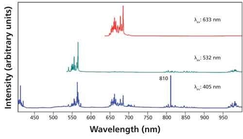
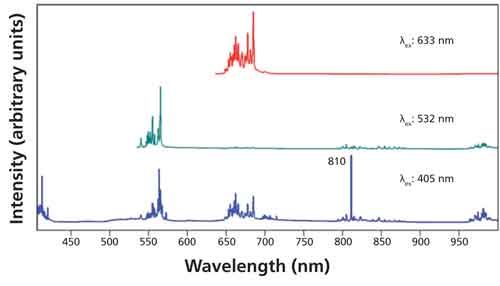
Figure 3: Photoluminescence spectra acquired from Er2O3 using excitation wavelengths of 405 nm (blue spectrum), 532 nm (green spectrum), and 633 nm (red spectrum).

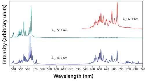

Figure 4: Photoluminescence spectra acquired from Er2O3 using excitation wavelengths of 405 nm (blue spectrum), 532 nm (green spectrum), and 633 nm (red spectrum).
Photoluminescence in Nd-Doped Glass
Another lanthanide that should be quite familiar to spectroscopists is neodymium. The element Nd has a ground-state electron configuration of [Xe] 4f4 6s2. The Nd:YAG crystal is the source of the 1064-nm laser line that functions as the excitation in Fourier transform (FT) Raman spectroscopy. Frequency doubling the 1064-nm line produces the 532-nm laser line that is so commonly used now with dispersive Raman spectrometers. Of course, there are many other electronic transitions reported for Nd and those transitions can be narrow or broad depending on the electronic orbitals involved in the transitions and the degree to which they couple to the surrounding environment (8).
The electronic transitions of Nd have been well characterized and so glass doped with Nd is often used as a standard for spectral calibration. The Nd doped glass can appear faint to dark violet depending on the thickness of the glass and therefore its optical density. The violet color of the glass indicates that the Nd is very likely in the +3 oxidation state because Nd2O3 has the same faint violet color (9). When Nd is oxidized to form Nd2O3, the formal oxidation state of the neodymium atom becomes +3 and its electron configuration is now [Xe] 4f3. Consequently, 4f3 becomes the highest occupied molecular orbital of Nd3+. Photoluminescence spectra of Nd doped glass excited with 405-, 532-, and 633-nm laser light are shown in Figure 5. The spectra appear quite barren in contrast to those of Er2O3 in Figures 3 and 4. The Nd-doped glass spectra are quite similar for all excitation wavelengths consisting of a weak peak at approximately 800 nm and a cluster of three partially resolved bands in the region from approximately 850 to 920 nm. The sharp peak at 810 nm in the spectrum excited with 405 nm light is from the grating’s second-order diffraction of the 405-nm laser light. We can infer from the widths of these bands that the electronic transitions involved are highly coupled to the surrounding oxide environment. That is, the chemical interactions with the surrounding glass are probably similar to those of Nd2O3. That interpretation would certainly be consistent with the violet color of the glass. It is likely that these transitions involve 4f-5d orbitals of Nd3+ with strong coupling of the 5d orbital to the SiO2 glass.

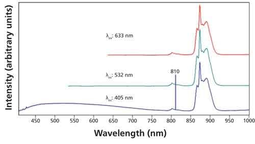
Figure 5: Photoluminescence spectra acquired from Nd doped glass using excitation wavelengths of 405 nm (blue spectrum), 532 nm (green spectrum), and 633 nm (red spectrum).
Raman Spectroscopy and Photoluminescence of 2D MoS2
The interest in two dimensional (2D) transition metal dichalcogenides (TMD) in general and MoS2 in particular is that a single layer of MoS2 atoms is a direct band gap semiconductor whereas the bulk form is an indirect band gap semiconductor. Thus, single-layer MoS2 emits light when illuminated with light whose energy is above the band gap. This property holds the promise of being able to fabricate electrooptic devices from single-layer MoS2 or other TMDs and has therefore been the subject of intense research and development over the past few years.
The crystalline structure of 2H-MoS2 belongs to the D6h crystal class, and factor group analysis predicts one A1g, one E1g, and two E2g Raman active modes (10–16). The symmetry assignments and corresponding Raman band positions for bulk hexagonal MoS2 are E1g (286 cm-1), E12g (383 cm-1), A1g (408 cm-1), and E22g (32 cm-1). Furthermore, it is important to remember that some visible wavelengths of the laser light used to excite Raman scattering correspond to energies of MoS2 electronic transitions. The absorption spectrum of MoS2 reflects the band gap of 1.7 eV, but it also manifests fine structure with narrow absorption peaks at 1.9 eV (653 nm) and 2.1 eV (590 nm) related to d-to-d orbital transitions split by spin-orbit coupling and designated A1 and B1 excitons, respectively (10,17). Consequently, one can observe an excitation wavelength dependence of the first-order Raman band intensities as well as the appearance of Raman bands assigned to harmonic and combination modes when the laser excitation is of a wavelength that couples into these excitonic transitions (10,14,16,17).
Exfoliated few-layer flakes of MoS2 are typically heterogeneous, and so the Raman and photoluminescence spectra tend to spatially vary on the flake. The effect of excitation wavelength on the photoluminescence spectra of few-layer MoS2 flakes can be seen in the spectra shown in Figure 6. The spectra were acquired at the same location on the flake and are plotted on arbitrary intensity scales to better show the differences in relative strengths of both the photoluminescence and Raman signals. There are several differences to observe that relate to the electronic transitions and their coupling to the few-layer MoS2 flake phonons. The photoluminescence excited at 532 nm is substantially weaker relative to the Raman scattering when compared to the photoluminescence/Raman strength ratio of the 632.8-nm-excited spectrum. Furthermore, the relative strengths of the 691- and 930-nm emissions are inverted for the 532- and 632.8-nm excitation wavelengths. An important aspect of this measurement is that one can simultaneously obtain a Raman spectrum and a photoluminescence spectrum from the same location. That fact holds important implications for the ability to simultaneously perform photoluminescence and Raman spectroscopy and imaging of few-layer MoS2 and other TMD 2D crystals, thereby supporting the research and development of these materials to the level of electrooptic devices.

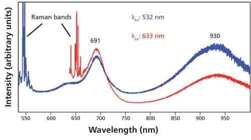

Figure 6: Photoluminescence and Raman spectra of few-layer MoS2 flake taken at the same location with different excitation wavelengths.
Conclusion
The high spectral resolution of a Raman spectrometer allows one to resolve narrow and closely spaced emissions from electronic transitions. Consequently, using a Raman spectrometer designed to resolve bands arising from vibrational modes and separated by wavenumbers in units of cm-1
is ideal for the detection of narrow band photoluminescence. Such spectral resolution may not be necessary for typical molecular fluorescence work; however, spectral resolution can be extremely important when working with solid-state materials. The free spectral range for photoluminescence when using a Raman spectrometer and CCD detector can extend from 400 nm to 1000 nm. Having the capability to perform photoluminescence and Raman spectroscopies simultaneously with the same instrument is advantageous, especially when studying 2D crystals. When used to perform photoluminescence spectroscopy, the Raman spectrometer becomes two instruments in one.
References
- D. Tuschel, Spectroscopy31(3), 14–23 (2016).
- K. Nassau, The Physics and Chemistry of Color: The Fifteen Causes of Color (Wiley-Interscience, New York, 1983), pp. 79–87.
- Q. Ma and D.R. Clarke, J.Am. Ceram. Soc. 77, 298–302 (1994).
- H. Mahiou, A. Beakou, and R.J. Young, J. Mat. Sci. 34, 6069–6080 (1999).
- W. Zhu and G. Pezzotti, Phys. Status Solidi A208, 1141–1150 (2011).
- W. Zhu and G. Pezzotti, J. Raman Spectrosc. 42, 2015–2025 (2011).
- G. Blasse and B.C. Grabmaier, Luminescent Materials (Springer-Verlag, New York, 1994), pp. 112–132.
- W.T. Carnall, G.L. Goodman, K. Rajnak, and R.S. Rana, J. Chem. Phys. 90, 3443–3457 (1989).
- G. Blasse and B.C. Grabmaier, Luminescent Materials (Springer-Verlag, New York, 1994), p. 26.
- J.R. Ferraro, Appl. Spec.29, 418–421 (1975).
- S. Jimenez Sandoval, D. Yang, R.F. Frindt, and J.C. Irwin, Phys. Rev. B44, 3955–3962 (1991).
- T.J. Wieting and J.L. Verble, Phys. Rev. B3, 4286–4292 (1971).
- J.M. Chen and C.S. Wang, Solid State Commun.14, 857–860 (1974).
- S. Sugai and T. Ueda, Phys. Rev. B26, 6554–6558 (1982).
- D.O. Dumcenco, K.Y. Chen, Y.P. Wang, Y.S. Huang, and K.K. Tiong, J. Alloys Compounds506, 940–943 (2010).
- B.C. Windom, W.G. Sawyer, and D.W. Hahn, Tribol. Lett. 42, 301–310 (2011).
- Y. Zhao, X. Luo, H. Li, J. Zhang, P.T. Araujo, C.K. Gan, J. Wu, H. Zhang, S.Y. Quek, M.S. Dresselhaus, and Q. Xiong, Nano Lett.13, 1007–1015 (2013).


David Tuschel is a Raman applications manager at Horiba Scientific, in Edison, New Jersey, where he works with Fran Adar. David is sharing authorship of this column with Fran. He can be reached at: SpectroscopyEdit@UBM.com


Newsletter
Get essential updates on the latest spectroscopy technologies, regulatory standards, and best practices—subscribe today to Spectroscopy.