|Articles|April 7, 2011
Banana Peel Used to Extract Metal Ions from River Water
Researchers use minced banana peel to extract lead and copper ions from raw river water.
Advertisement
Researchers from São Paulo State University (Ilha Solteira, Brazil) have used Fourier transform–infrared (FT-IR) spectrometry to examine the use of minced banana peel to extract lead and copper ions from water. Studying a sample of raw river water, the team applied FT-IR to the extraction of Cu(II) and Pb(II), which showed absorption bands of carboxylic and amine groups at 1730 and 889 cm1, respectively, and maximum adsorption capacities of 0.33 and 0.20 mmol g-1 for Cu(II) and Pb(II), respectively.
Led by Gustavo R. Castro of the Department of Crop Science, Food Technology, and Socioeconomics, the team applied the minced banana peel in the preconcentration system, which showed an enrichment factor of approximately 20-fold, and reused the column for 11 cycles without loss in the percentage of recovery. The team published their findings in the March 2011 issue of Industrial & Engineering Chemistry Research.
Advertisement
Related Content
Advertisement


Advertisement
Advertisement
Trending on Spectroscopy Online
1
When Political Appointees Outrank Peer Review: How a New Office of Management and Budget Rule Could Reshape Spectroscopy and Scientific Research Funding
2
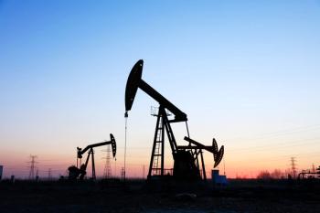
Is Produced Water a Source of Lithium?
3
The State of Spectroscopy Careers
4
Best of the Week: IR Spectral Interpretation, Women in STEM
5