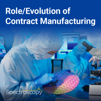
Experts explore the evolving role of CDMOs in semiconductor fabrication and why strategic partnerships are increasingly critical for process innovation and cost control.
Experts explore the evolving role of CDMOs in semiconductor fabrication and why strategic partnerships are increasingly critical for process innovation and cost control.

Looking ahead, panelists discuss emerging technologies, new analytical frontiers, and future regulatory pressures shaping semiconductor manufacturing over the next decade.
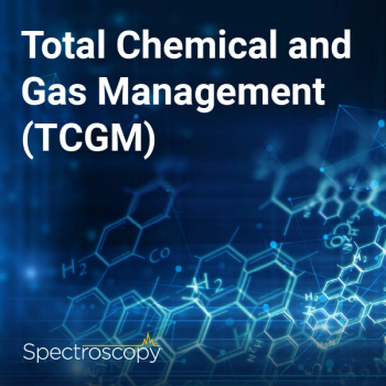
The panel takes a deep dive into total chemical and gas management (TCGM) strategies, and the growing need for online, real-time monitoring to protect yield and safety.

Panelists discuss cutting-edge advances in monitoring ultra-pure water (UPW) purity, from ICP-MS to online pre-concentration, and the growing push for sub-ppt-level contaminant detection.
The panelists discuss the vital role of ultra-pure water (UPW) and recycled water strategies to support yield, safety, and environmental compliance.

The panel discusses how silicon (Si), silicon carbide (SiC), and gallium nitride (GaN) materials influence semiconductor design choices, yield challenges, and supply chain risks.
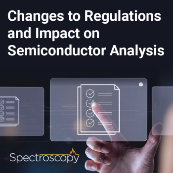
This episode takes a look at the evolving regulatory environment in semiconductor manufacturing, including stricter contamination standards and the challenges of global compliance.
The panelists consider non-destructive wafer analysis using TXRF and complementary methods, and how combining techniques enables advanced defect and contamination mapping.
In this episode, the panel focuses on automation in semiconductor analysis, including sample prep innovations and the unique capabilities of next-generation ICP-MS systems.
The panel compares traditional ATD-GC-MS methods to emerging TOF-MS approaches for impurity and defect analysis, emphasizing speed and sensitivity advancements.
The panelists discuss the different techniques used for testing semiconductor materials—such as ICP-MS, VPD, GDI, and GED-ICP-MS—including which approaches the industry will adopt more moving forward.
Ruth Merrifield, PhD, discusses how continuous manufacturing can help control contamination as humans don’t have to touch the materials as often, or even at all. Katsu Kawabata also mentions how automation that supports continuous manufacturing can help reduce human exposure to chemicals that would otherwise be manually handled.
Panelists discuss primary bottlenecks in semiconductor manufacturing, from geopolitical supply chain issues to purity and talent gaps, and explore strategies to maintain innovation under pressure.

Experts from across the industry prepare to explore the critical efficiency hurdles semiconductor fabricators are facing today, introducing themselves and their backgrounds.